Metal gate structure of a field effect transistor and field effect transistor

A technology of field effect transistors and gate electrodes, which is applied in the direction of circuits, electrical components, semiconductor devices, etc., can solve the problems of degraded device performance, increase circuit resistance and capacitance delay, and achieve the effect of low gate resistance value

Inactive Publication Date: 2011-06-22
TAIWAN SEMICON MFG CO LTD
View PDF4 Cites 30 Cited by
  • Summary
  • Abstract
  • Description
  • Claims
  • Application Information

AI Technical Summary

Problems solved by technology

Since the upper portion 128 with a lower resistance value only occupies a small portion of the area of ​​the multi-film metal gate electrode 120a, it can be observed that the multi-film metal gate electrode 120a will exhibit a higher gate Resistor value, which will increase the RC delay of the circuit and degrade the performance of the device

Method used


Image

  • Metal gate structure of a field effect transistor and field effect transistor
  • Metal gate structure of a field effect transistor and field effect transistor
  • Metal gate structure of a field effect transistor and field effect transistor

Examples


Embodiment Construction

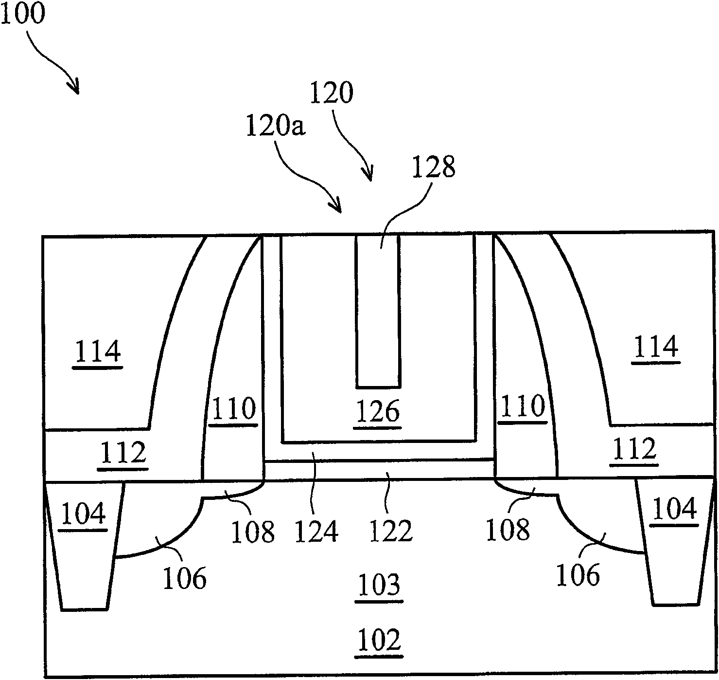
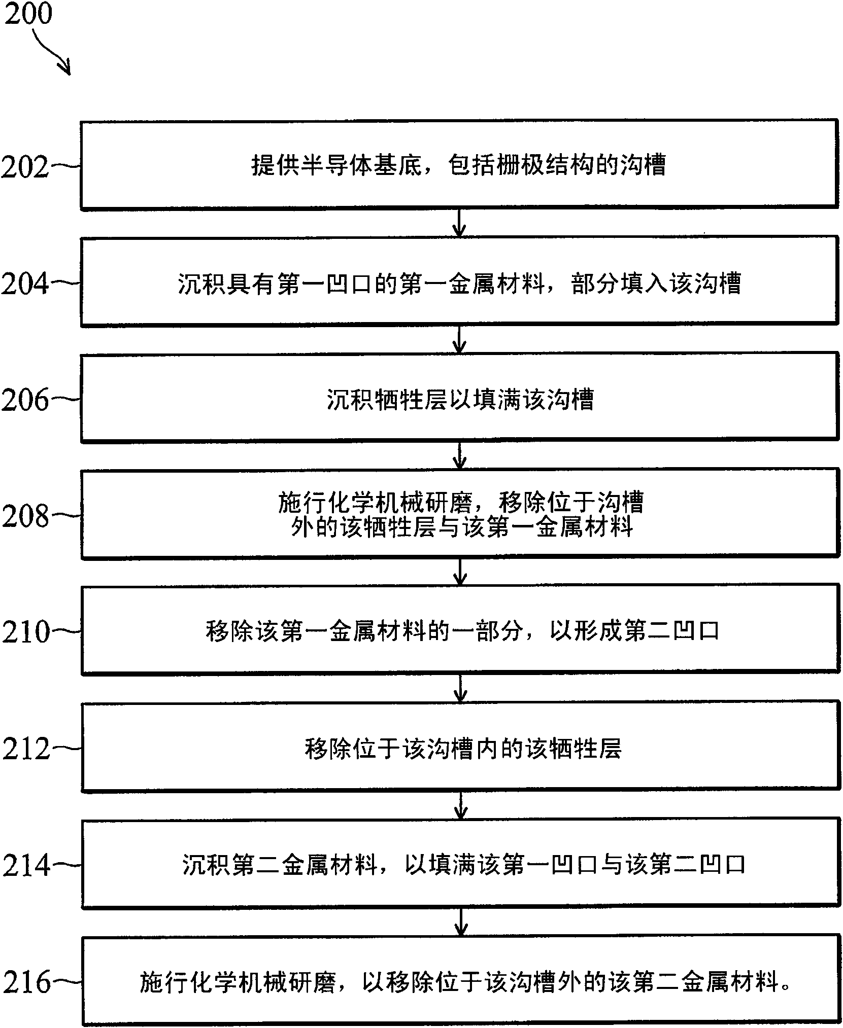
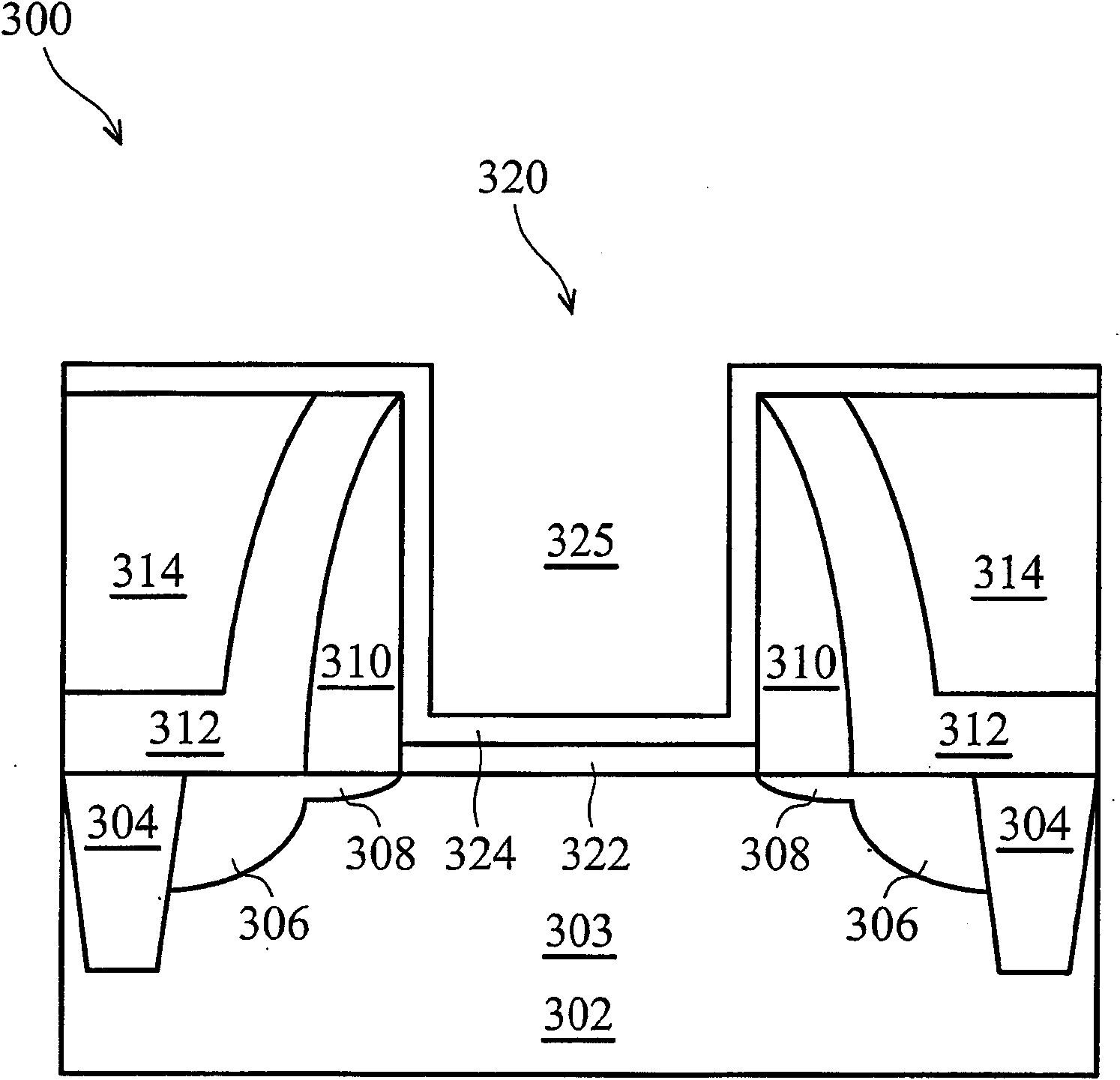
[0058] It will be appreciated that a number of different embodiments or examples are provided below to illustrate different features of the invention. To simplify the description of the present invention, specific examples of components and arrangements are described below. However, these examples are only used as examples and not intended to limit the present invention. For example, the formation of the first member on or over a second member may be a direct contact between the first member and the second member, and may also include a formation between the first member and the second member. The situation of the additional component, so that there may not be a direct contact situation between the first component and the second component. For the purpose of simplicity and clarity, different components may be arbitrarily shown in different scales. In addition, the present invention provides an example of a "gate last" metal gate process, but those skilled in the art can appl...


PUM


Abstract

The invention relates to integrated circuit fabrication, and more particularly to a Field Effect Transistor with a low resistance metal gate electrode. An exemplary structure for a gate electrode for a Field Effect Transistor comprises a lower portion formed of a first metal material having a recess and a first resistance; and an upper portion formed of a second metal material having a protrusion and a second resistance, wherein the protrusion extends into the recess, wherein the second resistance is lower than the first resistance. The metal gate electrode provided in the invention has a low gate resistance value, so can reduce the capacitance-resistance delay of circuit and improve the performance an apparatus.

Description

technical field [0001] The present invention relates to fabrication of an integrated circuit, and more particularly to a field effect transistor (FET) having a metal gate electrode. Background technique [0002] As transistor dimensions shrink, gate oxide thickness needs to be reduced to maintain performance with reduced gate length. However, in order to reduce gate leakage, a high-k gate dielectric film is used to maintain the same characteristics of known gate oxides used in larger technology nodes. It can have a higher physical thickness at an equivalent thickness. [0003] In addition, as technology nodes shrink, in some integrated circuit designs, metal gate electrodes need to be used to replace conventional polysilicon gate electrodes, so as to improve the performance of devices with reduced feature sizes. One of the processes for forming the metal gate is the "gate last" process, in which the metal gate is formed last, thus allowing the gate electrode to be protecte...

Claims


Application Information

Patent Timeline
Patent Type & Authority Applications(China)
IPC IPC(8): H01L29/423H01L29/49H01L29/78H01L21/28
CPCH01L21/823842H01L29/512H01L29/513H01L29/4983H01L29/517H01L29/4966H01L29/495H01L29/66545H01L21/28008
Inventor 林秉顺李达元许光源
Owner TAIWAN SEMICON MFG CO LTD
Why Eureka
Try Eureka