Method for Automatically Establishing Interlayer Error Measurement Programs in Batches in Photolithography Process

A lithography process and lithography layer technology, applied in the field of lithography, can solve problems such as increasing measurement time, and achieve the effects of reducing manufacturing time, improving efficiency, and reducing human operation errors

Active Publication Date: 2014-10-22
SHANGHAI HUAHONG GRACE SEMICON MFG CORP
View PDF3 Cites 0 Cited by
  • Summary
  • Abstract
  • Description
  • Claims
  • Application Information

AI Technical Summary

Problems solved by technology

However, most of the measurement programs need to be manually established on the silicon wafer, and each program must be created separately for each product, which not only introduces human error, but also increases the measurement time.

Method used


Image

  • Method for Automatically Establishing Interlayer Error Measurement Programs in Batches in Photolithography Process
  • Method for Automatically Establishing Interlayer Error Measurement Programs in Batches in Photolithography Process
  • Method for Automatically Establishing Interlayer Error Measurement Programs in Batches in Photolithography Process

Examples


Embodiment Construction

[0017] The present invention will be further described below in conjunction with the accompanying drawings and specific embodiments.

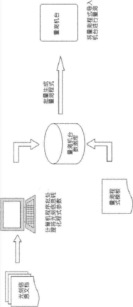
[0018] Such as figure 1 , a method for measuring an error between photolithography layers in a photolithography process, comprising the steps of:

[0019] 1) Make photolithographic information documents;

[0020] 2) Convert the lithographic information into a program parameter file;

[0021] 3) Create a template for a common measurement program, including

[0022] 3.1) A common reference pattern for product design;

[0023] First draw a reference pattern at a fixed position in the photomask design drawing as a mark for alignment and identification of the measuring machine; then import the reference pattern and its coordinates in the exposure area into the database of the measuring machine;

[0024] 3.2) Set common environmental parameters for product measurement;

[0025] 4) Import the program parameters into the database of the measuring ...


PUM


Abstract

A method for measuring an photoetching interlayer error in photoetching process includes steps as follows: (1) manufacturing a file about photoetching information; (2) converting the photoetching information into a program parameter file; (3) building a universal template about a measurement program; (4) inputting program parameters into a database of a measurement workbench, generating a measurement program corresponding to each product according to the template about the measurement program and the program parameters in the database, and finally using the measurement workbench for measuring the corresponding products; and (5) automatically integrating a photoetching interlayer error measurement program by the measurement workbench according to the generated files and the template. Compared with the prior art, the invention manufactures the file about the photoetching information, builds the template and writes computer programs; the measurement programs can be generated automatically in batch by using a computer; moreover, no silicon wafer is required, and the manual operation is avoided, so that the manufacturing time can be reduced, the efficiency can be improved, and the errors caused by manual operation are reduced.

Description

technical field [0001] The invention relates to the technical field of photolithography, in particular to a method for automatically batch-establishing interlayer error measurement programs in the photolithography process. Background technique [0002] Using a measuring machine to establish a measuring program to measure the error between photolithographic layers has been commonly used in the photolithographic process. However, most measurement programs need to be manually established on the silicon wafer, and each program must be established individually for each product, which not only introduces human error, but also increases the measurement time. Contents of the invention [0003] In order to solve the above-mentioned problems existing in the prior art, the present invention proposes a method for measuring the error between photolithography layers in the photolithography process, and the specific technical scheme is as follows: [0004] A method for measuring an erro...

Claims


Application Information

Patent Timeline
Patent Type & Authority Patents(China)
IPC IPC(8): G03F7/20
Inventor 岳力挽陆向宇陈骆
Owner SHANGHAI HUAHONG GRACE SEMICON MFG CORP
Why Eureka
Try Eureka