Semiconductor encapsulating method

A packaging method and semiconductor technology, applied in semiconductor/solid-state device manufacturing, electrical components, circuits, etc., can solve problems such as wire collapse, difficulty in changing design, failure of packaged products, etc., and achieve low manufacturing costs and equipment maintenance costs. The effect of wire collapse

Inactive Publication Date: 2011-06-29
UNIVERSAL SCIENTIFIC INDUSTRIAL (SHANGHAI) CO LTD
View PDF0 Cites 2 Cited by
  • Summary
  • Abstract
  • Description
  • Claims
  • Application Information

AI Technical Summary

Problems solved by technology

[0004] 1. It is not easy to change the design, that is, the design is relatively inelastic, especially in a small amount of production, which is not in line with economic benefits
[0005] 2. For tiny interconnect wires, the phenomenon of wire sweep will be caused by the melting and flow of the colloid during the molding process, which will cause a short circuit and make the subsequent packaging products invalid
[0006] 3. The cost of molds and corresponding equipment is relatively expensive, resulting in high manufacturing costs and equipment maintenance costs
[0007] 4. It will produce a lot of material waste, such as release glue, waste (Molding Compound), etc., causing environmental pollution, so it is not environmentally friendly

Method used


Image

  • Semiconductor encapsulating method
  • Semiconductor encapsulating method
  • Semiconductor encapsulating method

Examples


Embodiment Construction

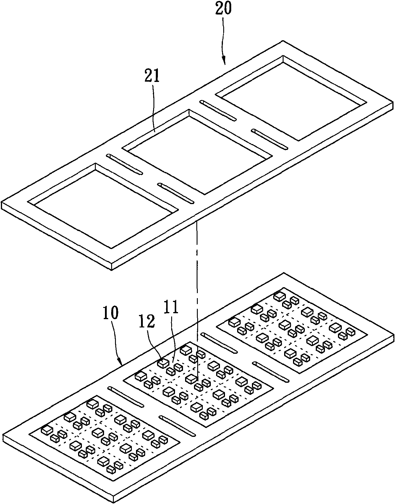
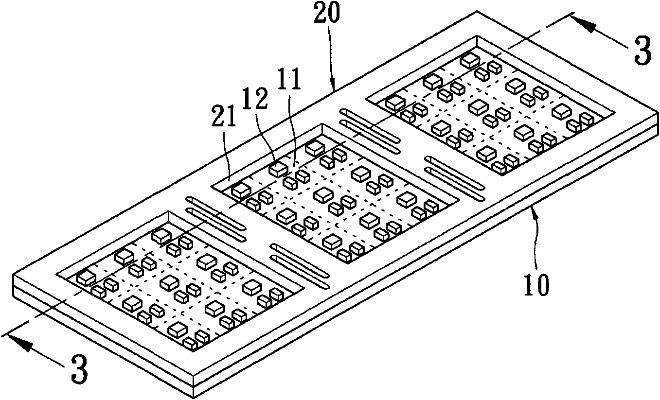
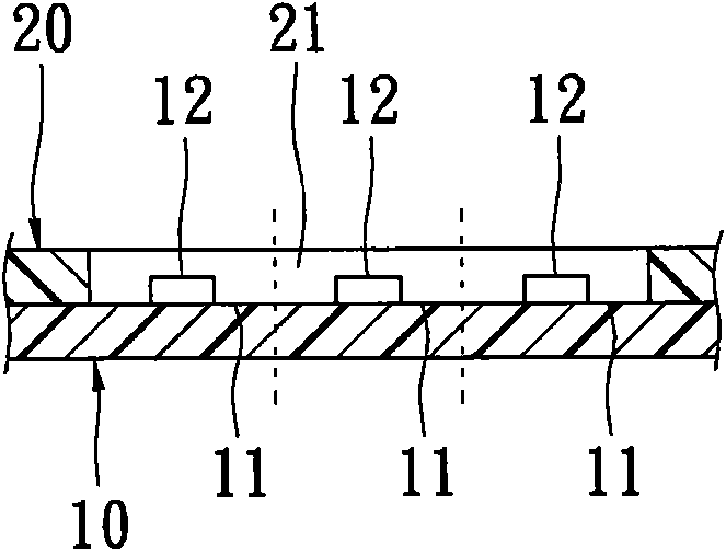
[0030] see figure 1 and figure 2 As shown, the present invention provides a semiconductor packaging method manufacturing method, which can be applied to various semiconductor packages, such as: System in Package Module (SIPModule). The manufacturing method includes the following steps:

[0031] (1) Prepare a substrate 10, which is divided into a plurality of packaging areas 11, and each packaging area 11 is provided with a plurality of electronic components 12 in an electrically connected manner. In the accompanying drawings, each packaging area 11 is provided with three electronic components. Take element 12 as an example. Wherein, the electronic component 12 can be determined according to the requirements of practical applications, and its type is not limited, and can be a chip, a passive component or a combination thereof. Wires (not shown in the figure) can be used to achieve electrical connection between the electronic component 12 and each package area 11 . In the d...


PUM


Abstract

The invention relates to a semiconductor encapsulating method which comprises the following steps: preparing a substrate, wherein the substrate is divided into a plurality of encapsulating regions, and each encapsulating region is provided with a plurality of electronic components in an electric connection mode; preparing a bare printed circuit board, wherein the bare printed circuit board is provided with a holding hole which penetrates through the upper and lower surfaces of the bare printed circuit board; pasting the bare printed circuit board onto the substrate, so that the bare printed circuit board encloses the encapsulating regions and the electronic components are held in the holding hole; and injecting a colloid into the holding hole of the bare printed circuit board to coat the electronic components. Thus, the semiconductor can be manufactured according to flexible designs, and can be suitable for small-scale production.

Description

technical field [0001] The invention relates to a semiconductor packaging method, in particular to a semiconductor packaging method that does not need to use a mold for sealing and is applicable to small-scale production. Background technique [0002] The current semiconductor packaging method is to perform packaging steps such as wire-bonding, sealing, and cutting of electronic components (such as chips) on a substrate. Among them, in the step of sealing glue, generally adopt the way of molding (Molding), that is to use the sealing mold to press on the substrate, and the cavity of the sealing mold covers all the electronic components correspondingly, so as to form a Independent padding space. Afterwards, the molten colloid (such as epoxy resin) is filled into the mold cavity. Next, after a high-temperature curing process, the glue is molded and the electronic components and the wires connected between the substrate and the electronic components are sealed. [0003] Howev...

Claims


Application Information

Patent Timeline
IPC IPC(8): H01L21/50H01L21/56
Inventor 许聪贤钟匡能
Owner UNIVERSAL SCIENTIFIC INDUSTRIAL (SHANGHAI) CO LTD
Why Eureka
Try Eureka