Method for reducing plasma induced damage in HDP CVD (high-density plasma chemical vapor deposition) process

A plasma and process technology, applied in the field of plasma-induced damage, can solve problems such as metal layer damage, poor yield and reliability of semiconductor devices, and impact, so as to improve yield and reliability, avoid direct bombardment, and reduce PID The effect of the phenomenon

Active Publication Date: 2011-06-29
SEMICON MFG INT (SHANGHAI) CORP +1
View PDF4 Cites 7 Cited by
  • Summary
  • Abstract
  • Description
  • Claims
  • Application Information

AI Technical Summary

Problems solved by technology

At this time, since the protective layer has not been deposited on the metal layer, when the wafer is bombarded with high-density plasma, the above-mentioned high-density plasma will directly bombard the metal layer, thus easily causing damage to the metal layer
[0026] It can be seen that, in the HDP CVD process in the prior art, the metal layer will still be greatly damaged, thereby adversely affecting the yield and reliability of the formed semiconductor device

Method used


Image

  • Method for reducing plasma induced damage in HDP CVD (high-density plasma chemical vapor deposition) process
  • Method for reducing plasma induced damage in HDP CVD (high-density plasma chemical vapor deposition) process
  • Method for reducing plasma induced damage in HDP CVD (high-density plasma chemical vapor deposition) process

Examples


Embodiment Construction

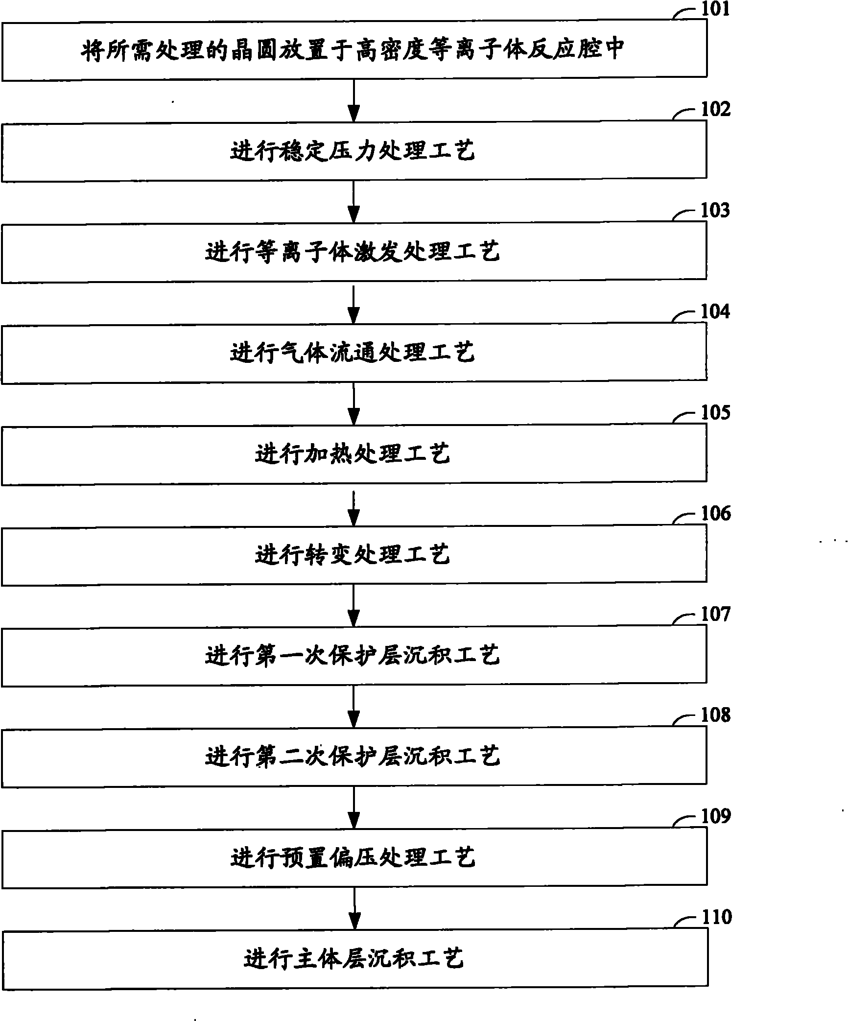
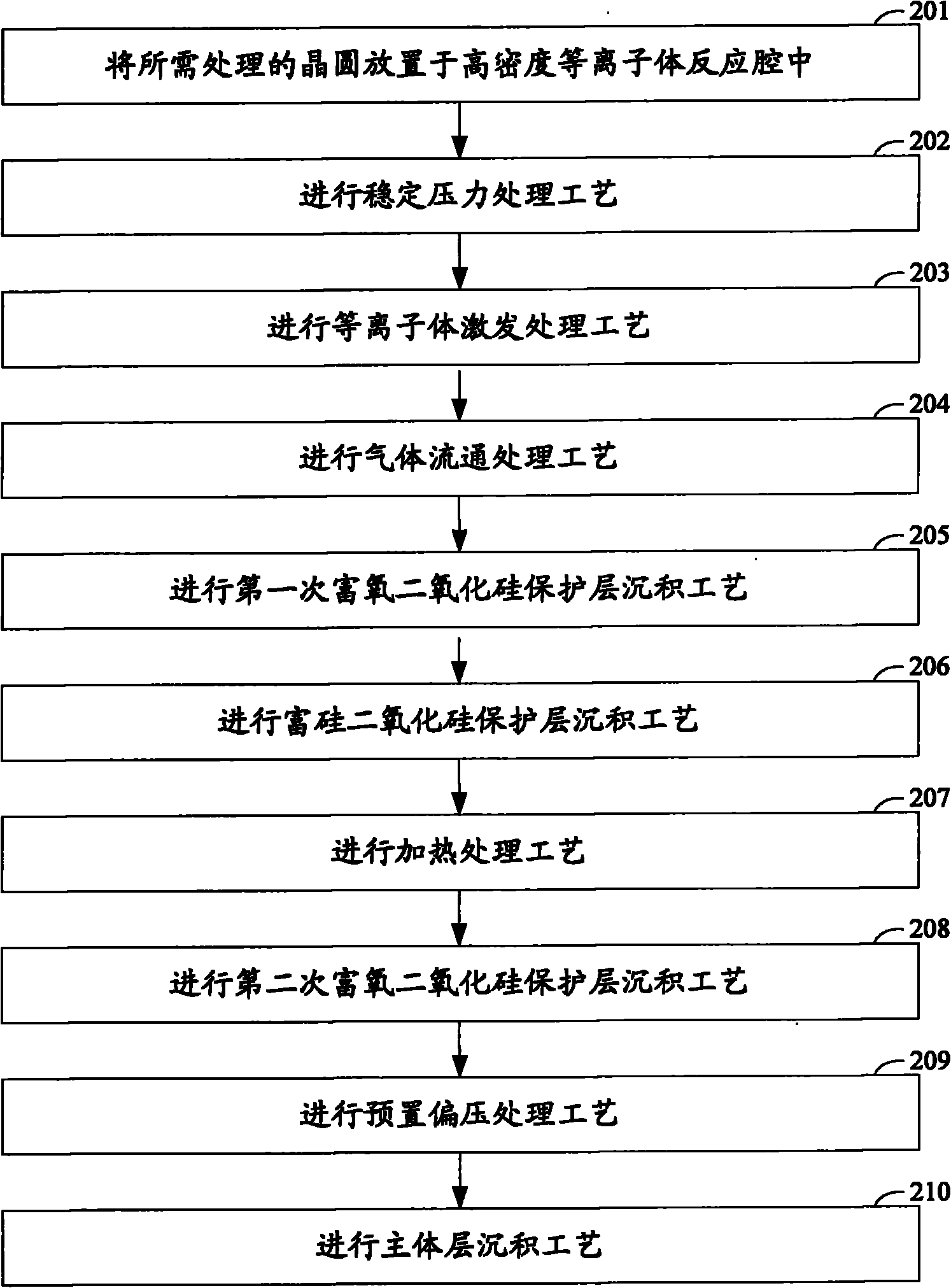
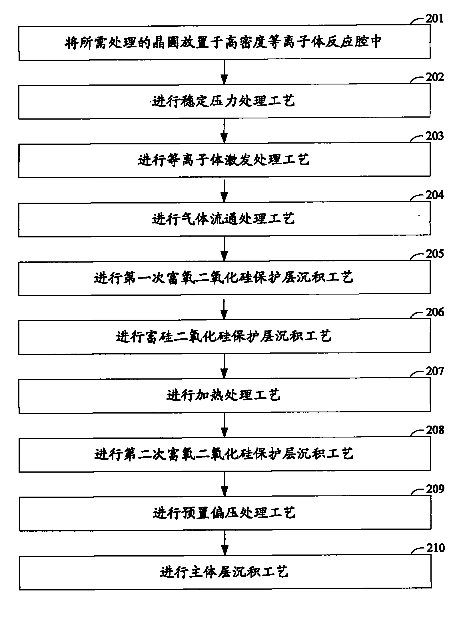
[0051] In order to make the objects, technical solutions and advantages of the present invention clearer, the present invention is described in further detail below with specific examples and with reference to the accompanying drawings.

[0052] figure 2 It is a flowchart of the HDP CVD process in the embodiment of the present invention. Such as figure 2 As shown, the HDP CVD process in the embodiment of the present invention includes the steps as follows:

[0053] Step 201, placing the wafer to be processed in a high-density plasma reaction chamber.

[0054] Step 202, performing a pressure stabilization process.

[0055] In this step, the reaction gas is fed into the high-density plasma reaction chamber, that is, the required reaction gas is input into the high-density plasma reaction chamber through the gas nozzle. This step lasts about 10 seconds, so that the pressure in the high-density plasma reaction chamber reaches a preset stable value. In an embodiment of the p...


PUM

PropertyMeasurementUnit
Thicknessaaaaaaaaaa

Abstract

The invention discloses a method for reducing plasma induced damage in an HDP CVD (high-density plasma chemical vapor deposition) process. The method comprises the following steps: putting a wafer needing to be processed in a high-density plasma reaction cavity to undergo a stable pressure treatment process, a plasma excitation treatment process and a gas circulation treatment process in sequence; carrying out a primary oxygen-enriched silicon dioxide protective layer deposition process; carrying out a silicon-enriched silicon dioxide protective layer deposition process to deposit a silicon-enriched silicon dioxide protective layer; carrying out a heating treatment process; and carrying out a secondary oxygen-enriched silicon dioxide protective layer deposition process, a preset bias voltage treatment process and a main layer deposition process in sequence. The method has the beneficial effects of effectively reducing the phenomenon of plasma induced damage and improving the yield andreliability of the semiconductor devices.

Description

technical field [0001] The invention relates to the field of semiconductor manufacturing, in particular to a method for reducing plasma-induced damage in a high-density plasma chemical vapor deposition (HDP CVD) process. Background technique [0002] With the rapid development of semiconductor manufacturing technology and the continuous improvement of the integration of large-scale integrated circuits, the density of active devices per unit area of ​​semiconductor substrates is getting higher and higher, and the distance between active devices is getting smaller and smaller. , so that the feature size of semiconductor devices can be significantly reduced. In the existing semiconductor manufacturing process with a process size of 65 nanometers or even smaller, the aspect ratio of the gap between semiconductor devices (that is, the ratio of the gap depth to the gap width) has reached 4:1 or higher, so that the insulation The homogeneous and non-porous filling process of the m...

Claims


Application Information

Patent Timeline
IPC IPC(8): H01L21/762H01L21/316
Inventor 徐强李敏吴永玉吴永坚
Owner SEMICON MFG INT (SHANGHAI) CORP
Why Eureka
Try Eureka