Multilayer wiring substrate

A multi-layer wiring substrate and copper layer technology, applied to electrical components, printed circuit components, printed circuits, etc., can solve problems such as insufficient connection strength and achieve reliable connection effects

Inactive Publication Date: 2011-06-29
NGK SPARK PLUG CO LTD
View PDF6 Cites 13 Cited by
  • Summary
  • Abstract
  • Description
  • Claims
  • Application Information

AI Technical Summary

Problems solved by technology

In addition, when soldering chip capacitors etc. to the connection terminals of electronic components, solder joints can only be formed on the upper surface of the terminals, which may result in insufficient connection strength.

Method used


Image

  • Multilayer wiring substrate
  • Multilayer wiring substrate
  • Multilayer wiring substrate

Examples


no. 1 Embodiment approach

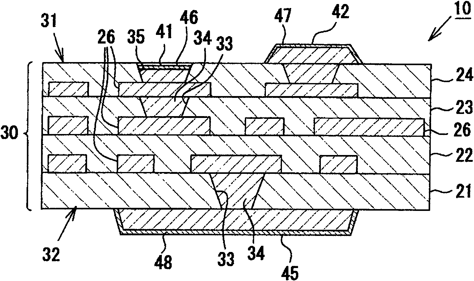
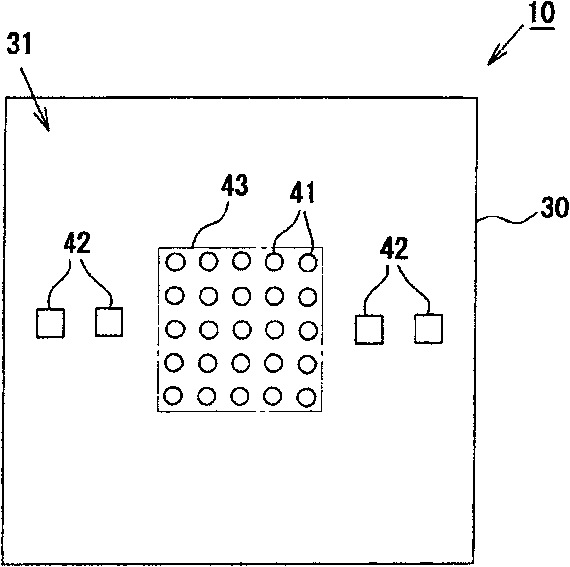
[0063] Hereinafter, a first embodiment in which the present invention is embodied as a multilayer wiring board will be described in detail with reference to the drawings. figure 1 is an enlarged cross-sectional view showing an outline of the structure of the multilayer wiring board according to the present embodiment, figure 2 is a plan view of the multilayer wiring board.

[0064] Such as figure 1 As shown, the multilayer wiring substrate 10 is a coreless wiring substrate formed without a core substrate, and has a wiring laminated portion 30 (laminated structure), which is composed of four resin insulating layers 21 mainly made of the same resin insulating material, 22 , 23 , 24 and the conductor layer 26 made of copper are alternately stacked in a multi-layered wiring laminated portion. Each of the resin insulating layers 21 to 24 is formed using a composite material mainly composed of a non-photocurable resin insulating material, specifically, a cured product of a thermo...

no. 2 Embodiment approach

[0098] Next, a second embodiment of the present invention will be described with reference to the drawings. Such as Figure 16 As shown, in the multilayer wiring board 10A of this embodiment, the shapes and manufacturing methods of the IC chip connection terminals 41A and capacitor connection terminals 42A formed on the upper surface 31 side of the wiring lamination portion 30 are the same as those of the above-mentioned first embodiment. different. The differences from the first embodiment will be described below focusing on the differences.

[0099] Such as Figure 16 As shown, in the multilayer wiring board 10A, no filled via conductor is formed in the opening 35 of the outermost resin insulating layer 24, and the height of the upper surface of the IC chip connection terminal 41A formed in the opening 35 is The height is substantially the same as that of the conductor layer 26 formed on the base pattern layer (resin insulating layer 23 ). In addition, a plated layer 46 ...


PUM


Abstract

A multilayer wiring substrate can reliably connect a plurality of connecting objects of different types. The multilayer wiring substrate is provided with a multilayer laminated structure (30) laminated alternately by a plurality of resin insulation layers (21-24) made primarily of the same resin insulation material, and a plurality of conductive layers (26), wherein on the upper surface (31) side of the laminated structure (30) there are provided an IC chip connector for connecting to IC chips, a capacitor connector (42) for connecting capacitors. The capacitor connector (42) is higher than a reference surface, and the IC chip connector (41) is lower than the reference surface, while the surface of the outermost resin insulation layers (24) exposed from the upper surface (31) of the laminated structure (30) is used as the reference surface.

Description

technical field [0001] The present invention relates to a multilayer wiring board having a multilayered laminate structure formed by alternately laminating a plurality of resin insulating layers and a plurality of conductor layers mainly made of the same resin insulating material, and not having a so-called core substrate. Background technique [0002] Semiconductor integrated circuit elements (IC chips) used as microprocessors of computers have been increasing in speed and functionality in recent years, the number of terminals attached to them has increased, and the pitch between terminals tends to decrease. Usually, a plurality of terminals are densely arranged in an array on the bottom surface of the IC chip, and this terminal group is flip-chip connected to the terminal group on the motherboard side. However, since the terminal group on the IC chip side and the terminal group on the motherboard side have a large difference in the pitch between the terminals, it is diffic...

Claims


Application Information

Patent Timeline
Patent Type & Authority Applications(China)
IPC IPC(8): H05K1/00H05K1/02
CPCH05K1/113H05K3/4682H05K2201/09472H05K2201/09427H05K3/4007H05K2201/094
Inventor 伊藤达也铃木哲夫半户琢也前田真之介杉本笃彦平野训
Owner NGK SPARK PLUG CO LTD
Why Eureka
Try Eureka