Full back side contact crystalline silicon cell and preparation method thereof

A back-contact, crystalline silicon cell technology, applied in circuits, photovoltaic power generation, electrical components, etc., can solve the problems of inability to take into account the movement of electrons and holes, increase the complexity of the process, and reduce the recombination of the battery body and the optical loss. , the effect of uniform doping energy and doping depth

Inactive Publication Date: 2014-07-02
DONGTAI HI TECH EQUIP TECH (BEIJING) CO LTD
View PDF12 Cites 7 Cited by
  • Summary
  • Abstract
  • Description
  • Claims
  • Application Information

AI Technical Summary

Problems solved by technology

[0007] However, in the existing full-back contact cell, the emitter and the base on the back made by ion implantation technology are in the same plane, which cannot allow electrons and holes to move to the emitter and base in a very short path.
In addition, the emitter and the base need to be insulated and isolated by laser etching, which increases the complexity of the process.

Method used


Image

  • Full back side contact crystalline silicon cell and preparation method thereof
  • Full back side contact crystalline silicon cell and preparation method thereof
  • Full back side contact crystalline silicon cell and preparation method thereof

Examples


Embodiment 1

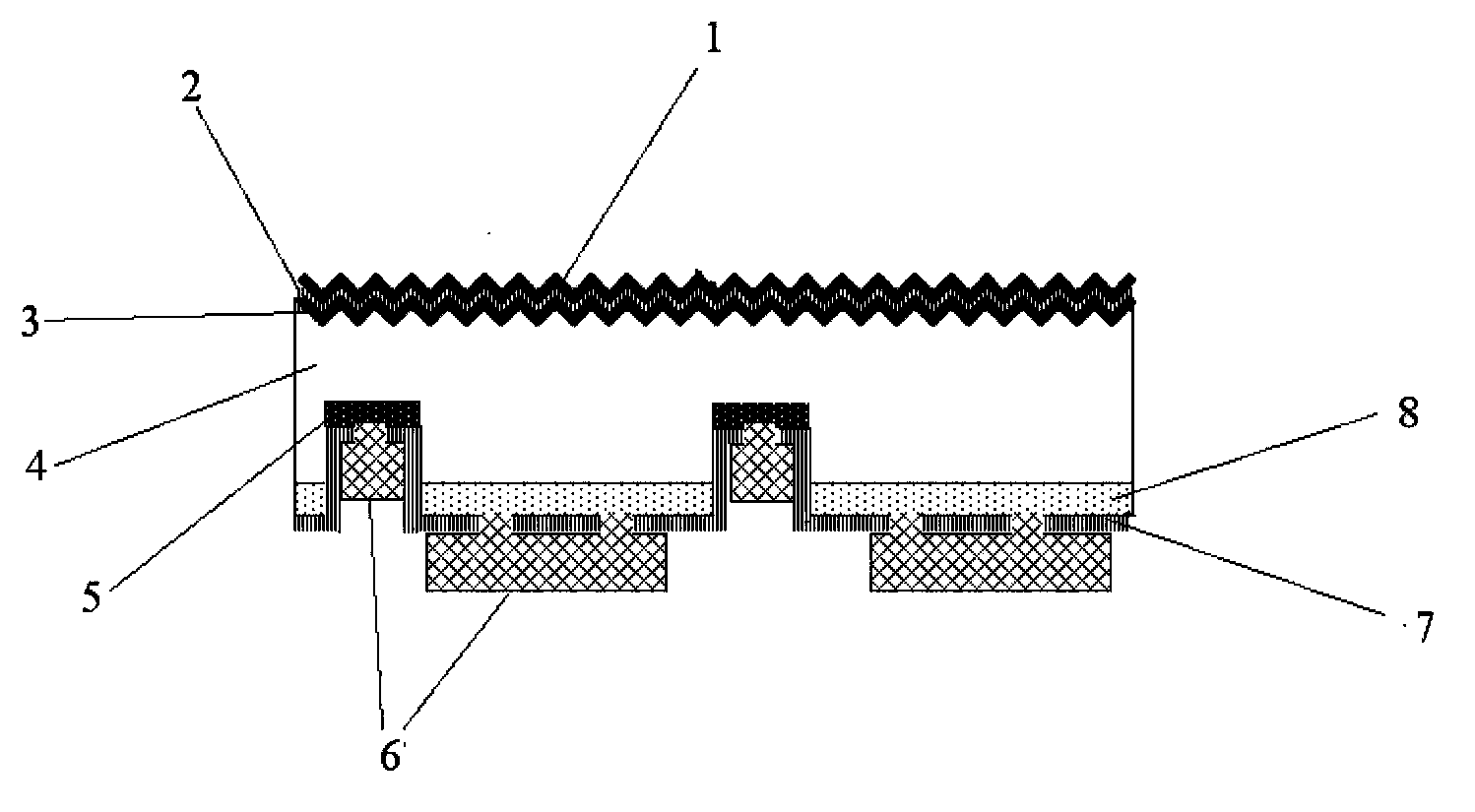
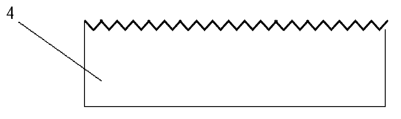
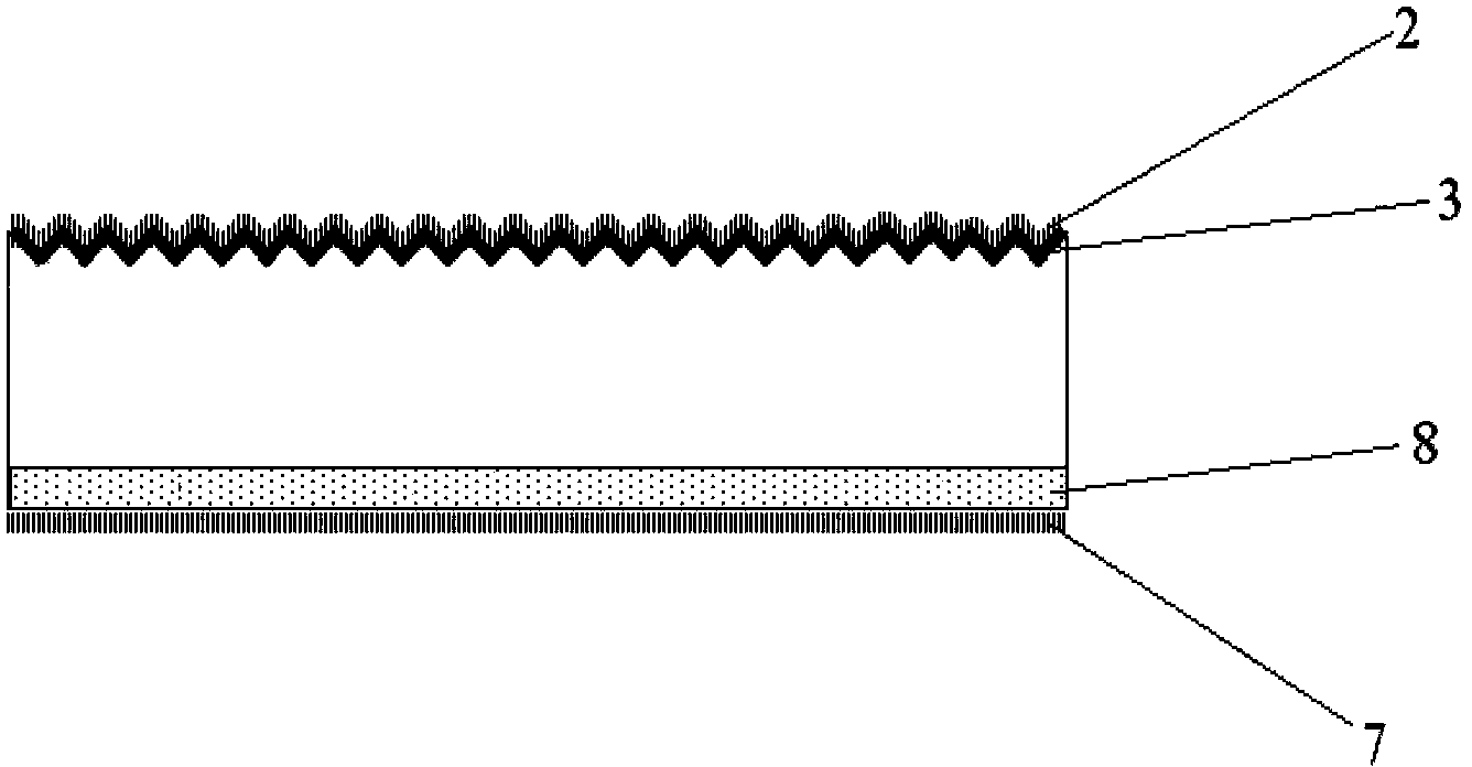
[0036] A full back contact crystalline silicon cell, such as figure 1 As shown, the battery includes: an n-type silicon substrate 4 with a thickness of 200 μm, a minority carrier lifetime of 1000 microseconds, and a resistance of 50 ohm / square. The reverse layer 1, the front oxide layer 2, the front surface electric field FSF3 formed by the lightly doped region on the front surface, and the silicon substrate 4. On the back side, there are P+ emitters 8 formed by non-patterned heavily doped regions, patterned grooves, and n+ bases 5 formed by patterned heavily doped regions at the bottom of the grooves. There is a rear oxide layer 7 on the back, and there are openings in the oxide layer in the regions of the emitter 8 and the base 5, and metal grid lines 6 are formed in the opening regions of the emitter 8 and the base 5 to connect, and the metal connections of different poles are insulated disconnect.

[0037] For the preparation method of full back contact crystalline silic...

Embodiment 2

[0046] A full back contact crystalline silicon cell, such as figure 1 As shown, the battery includes: an n-type silicon wafer substrate 4 with a thickness of 160 μm, a minority carrier lifetime of 1000 microseconds, a resistance of 20 ohm / square, and a pyramid texture structure on the front light-receiving surface, which is covered with a light-receiving surface from top to bottom. The reverse layer 1, the front passivation layer 2, the n+ type front surface electric field FSF3 formed by the lightly doped region on the front surface, and the silicon substrate 4. On the back side, there are P+ emitters 8 formed by non-patterned heavily doped regions, patterned grooves, and n+ bases 5 formed by patterned heavily doped regions at the bottom of the grooves. There is a back passivation layer 7 on the back, and there are openings in the passivation layer in the region of the emitter 8 and the base 5, and metal grid lines 6 are formed in the opening regions of the emitter 8 and the b...


PUM


Abstract

The invention relates to a novel crystalline silicon cell in the field of a photovoltaic technology, and specifically relates to a full back side contact crystalline silicon cell which is prepared through combination with an ion implantation technology, and also relates to a preparation method of the cell. The full back side contact crystalline silicon cell comprises a silicon chip substrate, an anti-reflection layer, a base electrode, an emitter electrode, a metal gate line and the like. The emitter electrode and the base electrode of the full back side contact crystalline silicon cell are not disposed in the same plane, so that electrons and cavities can be considered to move to the emitter electrode and the base electrode through a quire short path, and carrier bulk recombination in the cell can be reduced; through moving the emitter electrode and the metal grate line from a front surface, i.e., a light receiving surface to a back surface, the optical loss is reduced; the emitter electrode is obtained through an ion implantation method, and the process steps are reduced compared to a conventional thermal diffusion doping method; and the front surface and the back surface are each provided with a passivation layer, and the front surface is further provided with a front surface field (FSF), so that the carrier surface recombination can be reduced, and the invention finally provides a solar cell which has the advantages of high batch production efficiency and simple technology.

Description

technical field [0001] The invention relates to a new type of crystalline silicon battery in the field of photovoltaic technology, in particular to a full-back contact crystalline silicon battery combined with ion implantation technology; the invention also relates to a preparation method of the battery. Background technique [0002] Photovoltaic technology is a technology that uses a pn junction diode to convert solar energy into electrical energy. This pn junction diode is what we usually call a solar cell. When the solar cell is irradiated by the sun, the photons generate electron-hole pairs in the solar cell, and the pn junction separates the electron-hole pairs, which can form a current through an external circuit connection, thereby outputting power to the outside. [0003] Solar cells can be divided into crystalline silicon solar cells and thin-film solar cells. The emitter contact electrodes and base contact electrodes of traditional crystalline silicon cells are mad...

Claims


Application Information

Patent Timeline
Patent Type & Authority Applications(China)
IPC IPC(8): H01L31/0224H01L31/18
CPCH01L31/022441Y02E10/50Y02P70/50
Inventor 彭东阳张庆钊丁建
Owner DONGTAI HI TECH EQUIP TECH (BEIJING) CO LTD
Why Eureka
Try Eureka