
Method for manufacturing solar cell

A technology for solar cells and manufacturing methods, applied in the direction of final product manufacturing, sustainable manufacturing/processing, circuits, etc., can solve problems such as increased processes and damage to photoelectric converters, and achieves reduction in the number of processes, suppression of adverse effects, and photoelectric conversion efficiency. excellent effect

Inactive Publication Date: 2011-06-29
ULVAC INC
View PDF1 Cites 2 Cited by
  • Summary
  • Abstract
  • Description
  • Claims
  • Application Information

AI Technical Summary

Problems solved by technology

In order to remove these three layers, it is necessary to irradiate the laser multiple times, thus resulting in an increase in the process
Furthermore, the photoelectric converter of the solar cell may be damaged

Method used


Image

  • Method for manufacturing solar cell
  • Method for manufacturing solar cell
  • Method for manufacturing solar cell

Examples


Embodiment Construction

[0031] Hereinafter, one embodiment of the method for manufacturing a solar cell according to the present invention will be described with reference to the drawings. In addition, this embodiment is concretely demonstrated for better understanding of the gist of the invention, and does not limit this invention unless it specifies otherwise. In addition, in the drawings used in the following description, in order to facilitate understanding of the characteristics of the present invention, main parts may be shown enlarged for convenience, and the dimensional ratio of each component is not necessarily the same as the actual one.

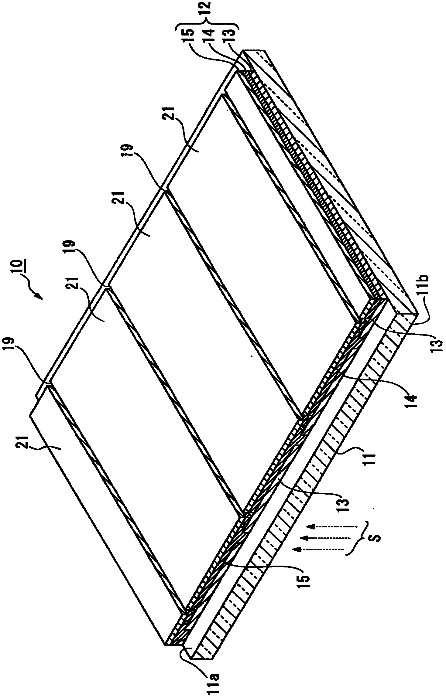
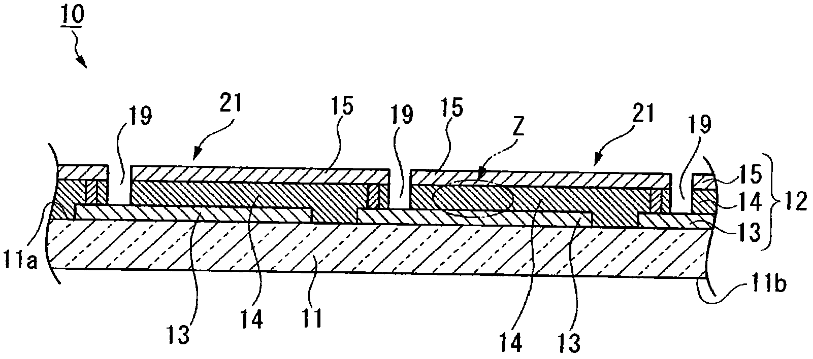
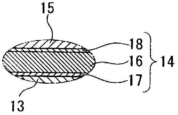
[0032] figure 1 It is an enlarged perspective view of main parts showing an example of an amorphous silicon solar cell manufactured by the method for manufacturing a solar cell of the present invention. in addition, Figure 2A is showing figure 1 A partial cross-sectional view of the layer structure of a solar cell. The solar cell 10 has a transpare...


PUM


Abstract

Provided is a method for manufacturing a solar cell wherein a photoelectric conversion body, which has a first electrode layer, a semiconductor layer and a second electrode layer stacked therein in this order, is formed on one surface of a substrate, a connecting portion between the first electrode layer and the second electrode layer is provided, the photoelectric conversion body has a plurality of separated elements which are electrically separated by scribe lines having the semiconductor layer and the second electrode layer removed therefrom, and the separated elements adjacent to each other are electrically connected. The method is provided with a defective region specifying step of specifying a region where a structural defect of the photoelectric conversion body exists, and a repair step of removing or separating the structural defect by irradiating the photoelectric conversion body with a laser beam, forming three repair lines each of which has the semiconductor layer and the second electrode layer removed therefrom, and surrounding the region where the structural defect exists by using the three repair lines and the one scribe line. In a region alpha including a contact section where the semiconductor layer is in contact with the substrate in alpha region between the structural defect and the connecting section in the photoelectric conversion body, one repair line among the three repair lines is formed.

Description

technical field [0001] The present invention relates to a method of manufacturing a solar cell. More specifically, the present invention relates to the manufacture of a solar cell capable of removing and separating a structural defect region from a normal region by removing a semiconductor layer and a second electrode layer with a laser to form a repair line and by using the repair line and the scribe line. method. More specifically, the present invention relates to a method of manufacturing a solar cell capable of minimizing reduction in photoelectric conversion efficiency by minimizing the area used to remove and separate structural defect regions from normal regions. [0002] This application claims priority based on Japanese Patent Application No. 2008-222171 for which it applied in Japan on August 29, 2008, and uses the content here. Background technique [0003] From the viewpoint of efficient energy utilization, solar cells have been widely and widely used in recent...

Claims


Application Information

Patent Timeline
Patent Type & Authority Applications(China)
IPC IPC(8): H01L31/04
CPCH01L27/1423Y02E10/50H01L31/208H01L31/186H01L31/046Y02P70/50
Inventor 山室和弘汤山纯平山根克巳
Owner ULVAC INC
Learn More