
Resistance-change non-volatile memory device

A non-volatile storage, resistance change technology, applied in information storage, static storage, digital storage information, etc., can solve the problems of inability to read the same performance, hindering low voltage, and increasing the complexity of the chip area.

Active Publication Date: 2011-07-06
PANASONIC SEMICON SOLUTIONS CO LTD
View PDF13 Cites 8 Cited by
  • Summary
  • Abstract
  • Description
  • Claims
  • Application Information

AI Technical Summary

Problems solved by technology

However, since the writing resistance value is different from the desired resistance value, the reading performance cannot be made uniform, and as a result, there is a problem that a product with stable performance cannot be provided.
In addition, since a high voltage is required, there is also a problem of hindering the reduction of voltage, or a second problem described later.
[0049] In addition, it is conceivable that both the A mode and the B mode may appear, and both the LR driving circuit and the HR driving circuit are prepared as both the word line driving circuit and the bit line driving circuit. The method of switching according to the appearance state of the B mode, but there are problems related to the complexity of switching settings according to the state, or the increase of the chip area.
[0050] The second problem is related to the reliability of the memory cell, especially the current control element
[0052] When the A-mode and B-mode are contrary to assumptions, as described in the first problem, by applying a high voltage and supplying more current during the high-resistance high-resistance operation, the high-resistance operation can be performed, but there are Possibility of deteriorating diode characteristics

Method used

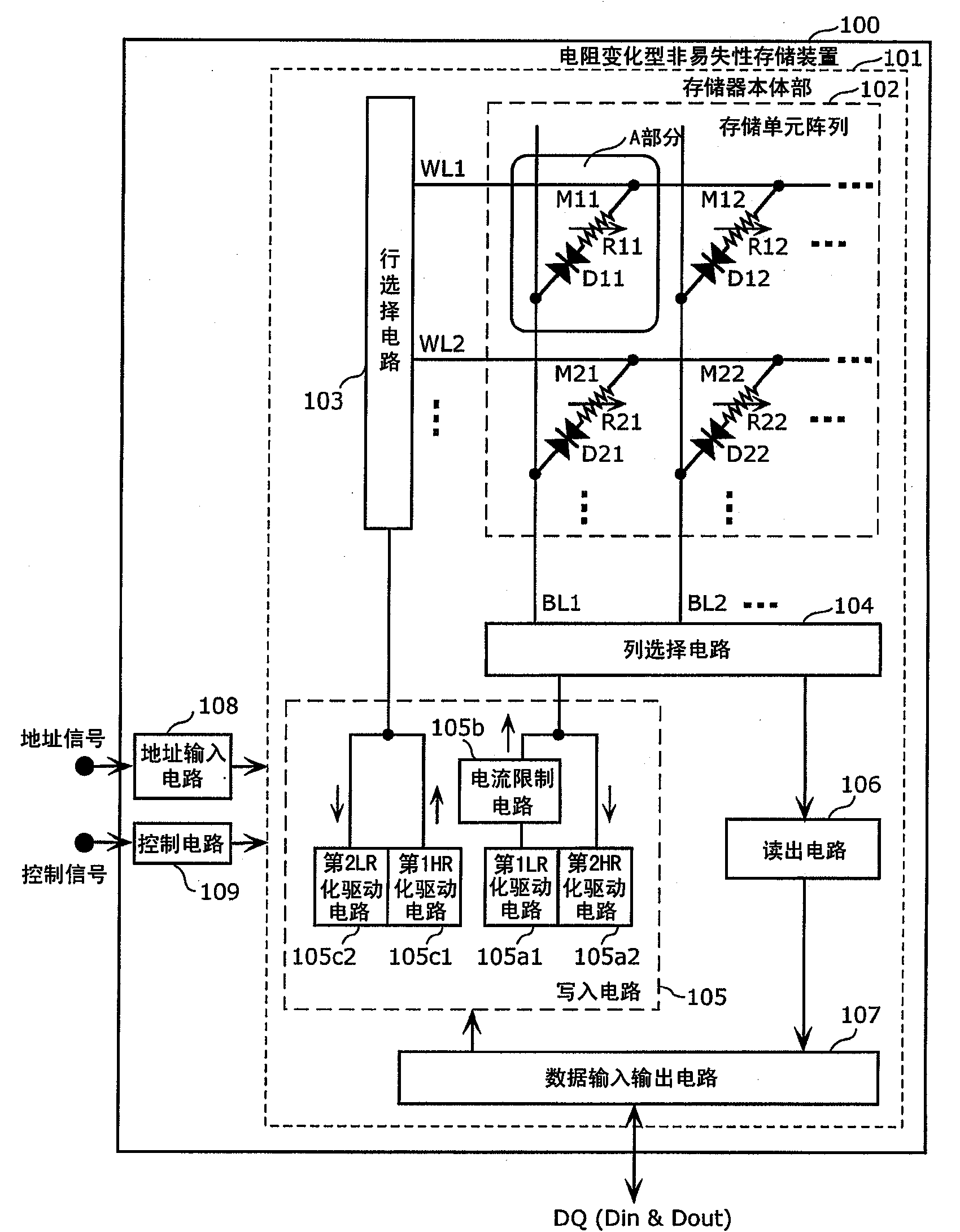
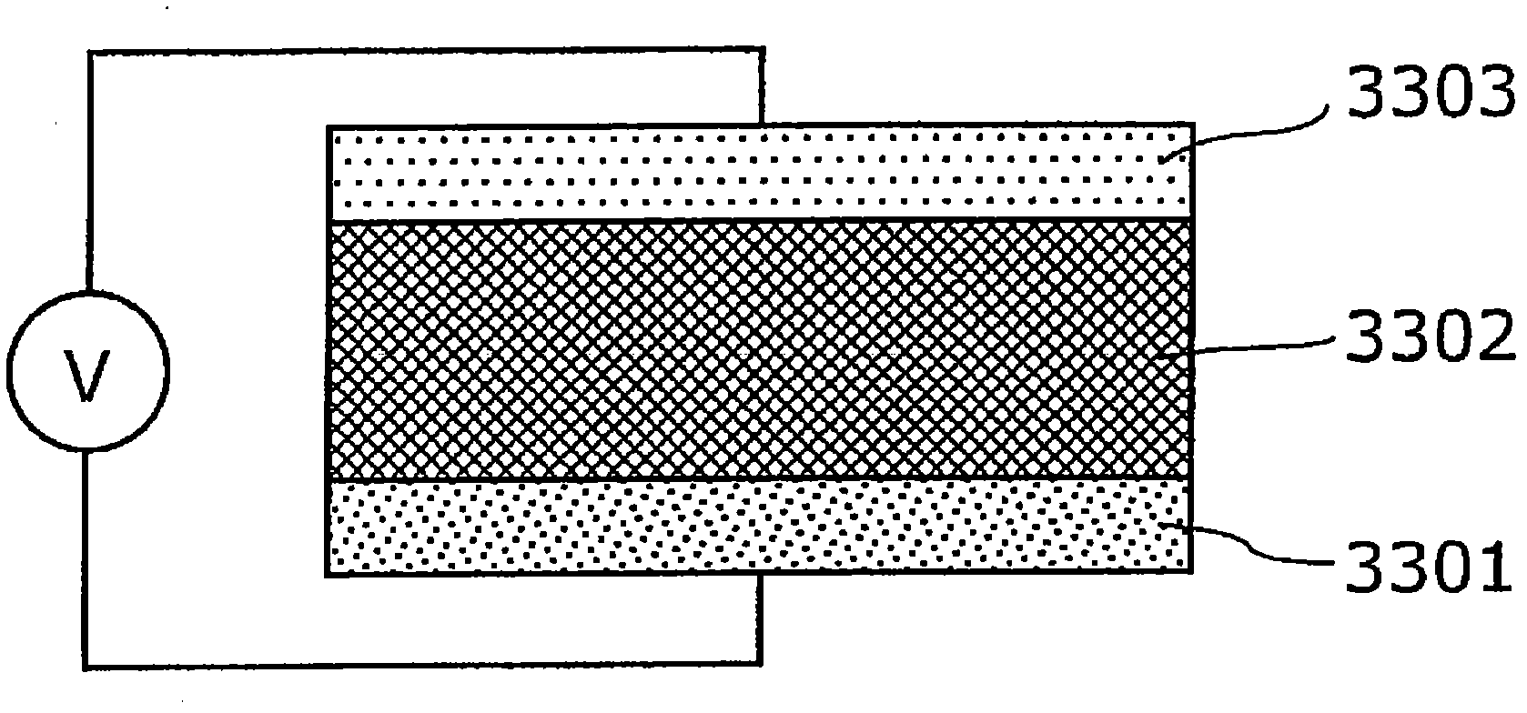
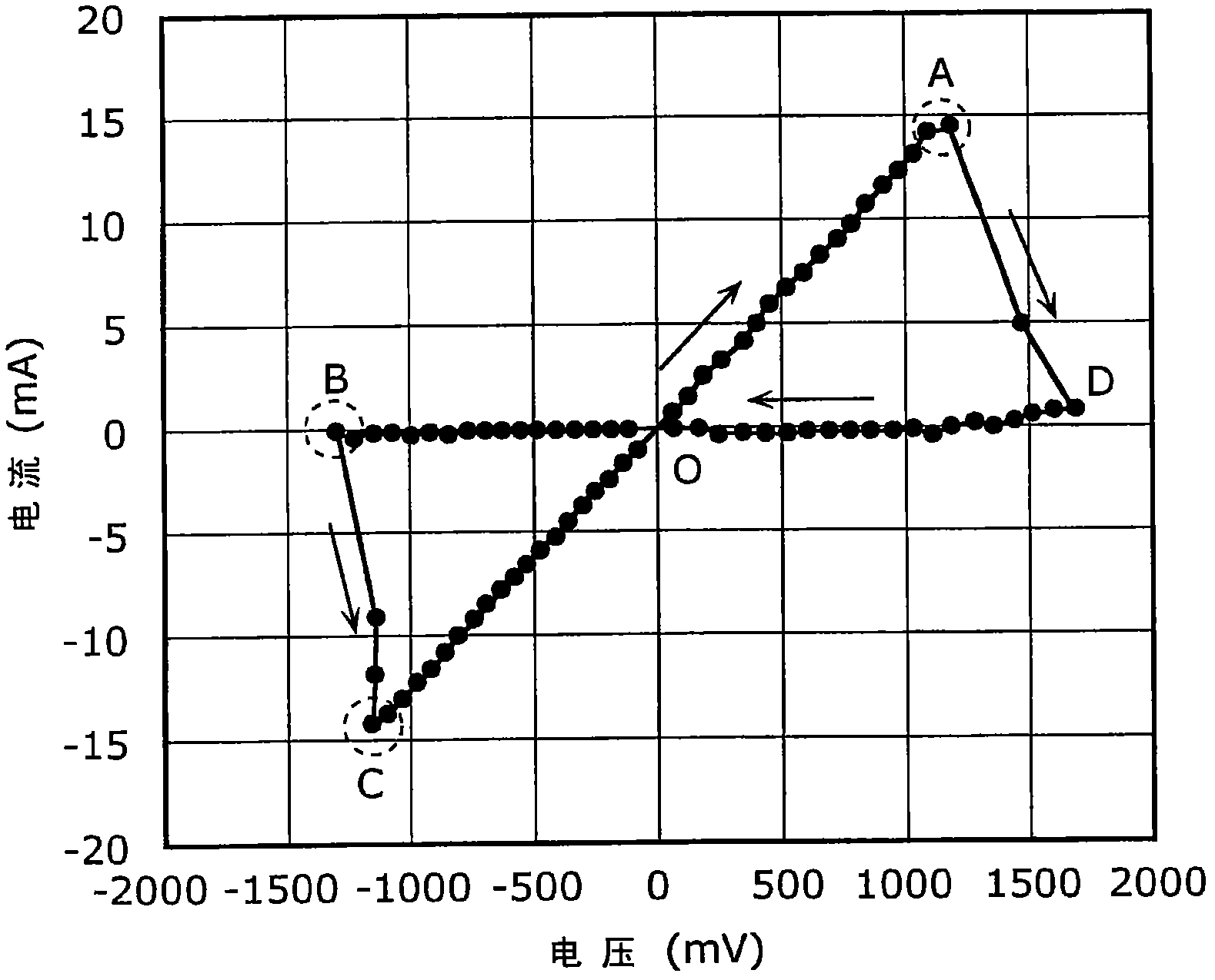

Image

  • Resistance-change non-volatile memory device
  • Resistance-change non-volatile memory device
  • Resistance-change non-volatile memory device

Examples


Embodiment Construction

[0107] Hereinafter, embodiments of the present invention will be described in detail with reference to the drawings.

[0108] The variable resistance nonvolatile memory device according to the embodiment of the present invention is a cross-point nonvolatile memory device using a plurality of 1D1R type memory cells connected in series to a variable resistance element and a current steering element. The pattern of the resistance variable characteristic of the resistance variable element, and the structure of the driving circuit is optimized according to the fixed pattern.

[0109] [Basic data of the present invention]

[0110] As a preparation, basic data related to two types of variable resistance materials used in the variable resistance element of the variable resistance nonvolatile memory device of the present invention will be described.

[0111] These variable resistance elements are composed of upper and lower electrodes made of different materials, respectively sandwich...


PUM


Abstract

A resistance-change non-volatile memory device (100) is provided with memory cells (M11, M12,...), each comprising a resistance-change element (R11, R12,...) and a current control element (D11, D12,...) connected in series. The resistance-change elements constitute a resistance-change layer interposed between a first electrode and a second electrode and provided so as to contact both electrodes. The current control elements constitute a current control layer interposed between a third electrode and a fourth electrode and provided so as to contact both electrodes. To decrease the resistance of the resistance-change elements, said elements are driven by a first LR drive circuit (105a1), via a current control circuit (105b). To increase the resistance of the resistance-change elements, the elements are driven by a second HR drive circuit (105a2). The current control circuit (105b) makes the current lower when decreasing the resistance of the resistance-change elements than when increasing the resistance thereof.

Description

technical field [0001] The present invention relates to a variable resistance nonvolatile memory device including a memory cell including a variable resistance element whose resistance value changes reversibly based on an electric signal, and a current control element. Background technique [0002] In recent years, research and development of a nonvolatile memory device having a memory cell constituted by a variable resistance element has progressed. The variable resistance element refers to an element that has a property that its resistance value changes reversibly according to an electrical signal, and can store data corresponding to the resistance value in a non-volatile manner. [0003] As a nonvolatile memory device using variable resistance elements, it is generally known that transistors and variable resistance elements connected in series, so-called A non-volatile memory device called a memory cell of the 1T1R type. In addition, it is known that diode elements and ...

Claims


Application Information

Patent Timeline
IPC IPC(8): G11C13/00H01L27/10H01L45/00
CPCG11C13/0069G11C2213/72H01L27/24G11C13/0007G11C2213/12G11C2213/15G11C2213/34G11C2013/0073H10B63/00
Inventor 池田雄一郎岛川一彦神泽好彦村冈俊作东亮太郎
Owner PANASONIC SEMICON SOLUTIONS CO LTD
Learn More