Solar cell and method for manufacturing same
A solar cell and manufacturing method technology, applied in the direction of circuits, photovoltaic power generation, electrical components, etc., can solve the problems of long PECVD process time, difficulty in meeting PECVD process conditions, and low productivity, so as to improve photoelectric conversion efficiency, shorten process time, The effect of saving the manufacturing unit price
- Summary
- Abstract
- Description
- Claims
- Application Information
AI Technical Summary
Problems solved by technology
Method used
Image
Examples
Embodiment approach
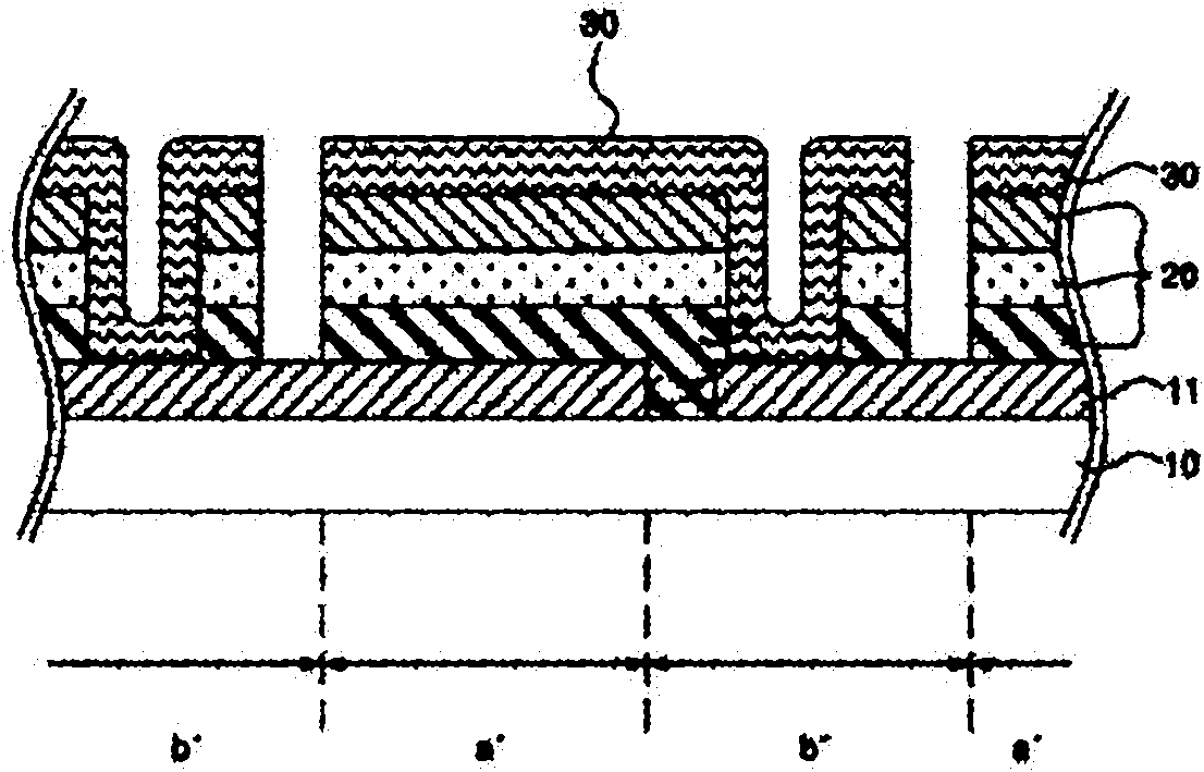
[0053] In order to achieve the above-mentioned object, the solar cell of the present invention includes: a substrate; a lower electrode formed on the substrate; a photovoltaic element part including a polycrystalline photovoltaic element formed on the lower electrode and laminated with a plurality of polycrystalline semiconductor layers, And an amorphous photovoltaic element formed on the polycrystalline photovoltaic element and laminated with a plurality of amorphous semiconductor layers; and an upper electrode formed on the photovoltaic element portion.
[0054] In addition, in order to achieve the above object, the method for manufacturing a solar cell according to the present invention includes: a step of forming a lower electrode on a substrate; and a step of forming a photoelectric element portion on the lower electrode, the photoelectric element portion including and A polycrystalline photovoltaic element laminated with a plurality of polycrystalline semiconductor layers, a...
Embodiment 1
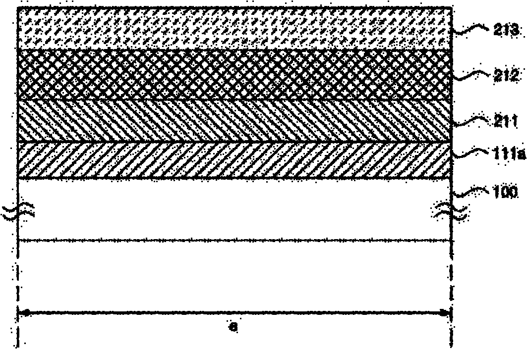
[0089] The structure of the unit area a of the tandem solar cell according to Example 1 of the present invention is the same as the structure of the unit area a of the tandem solar cell described above. Therefore, in Embodiment 1 below, detailed descriptions of the structural elements included in the unit area a are omitted in order to avoid overlapping descriptions.
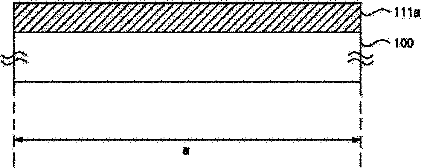
[0090] Figure 6 to Figure 11 It is a figure which shows the series connection type solar cell and its manufacturing method concerning Example 1 of this invention.
[0091] First, refer to Image 6 , A substrate 100 is provided, the substrate 100 includes a plurality of wiring areas b, and the plurality of wiring areas b are located between the plurality of cell areas a and the cell areas a.
[0092] At this time, an anti-reflection layer (not shown) may be additionally formed on the substrate 100 to prevent the incident sunlight from being directly reflected to the outside without being absorbed, resulting in a decrea...
Embodiment 2
[0108] The structure of the series connection type solar cell according to Example 2 of the present invention is the same as the series connection type solar cell of Example 1 except for the wiring area b. Therefore, in the following Embodiment 2, the description overlapping with Embodiment 1 is omitted.
[0109] Figure 12 to Figure 17 It is a figure which shows the series connection type solar cell and its manufacturing method concerning Example 2 of this invention.
[0110] First, refer to Picture 12 , A substrate 100 is provided, the substrate 100 includes a plurality of wiring areas b, and the plurality of wiring areas b are located between the plurality of cell areas a and the cell areas a.
[0111] Next, a lower conductive layer 110 made of a conductive material is formed on the substrate 100.
[0112] Next, refer to Figure 13 , The lower conductive layer 110 is patterned to form the lower electrode layer 111 (111a, 111b) of a predetermined pattern. That is, the lower electr...
PUM
 Abstract
Description
Claims
Application Information
 - R&D
- Intellectual Property
- Life Sciences
- Materials
- Tech Scout
- Unparalleled Data Quality
- Higher Quality Content
- 60% Fewer Hallucinations
Browse by: Latest US Patents, China's latest patents, Technical Efficacy Thesaurus, Application Domain, Technology Topic, Popular Technical Reports.
© 2025 PatSnap. All rights reserved.Legal|Privacy policy|Modern Slavery Act Transparency Statement|Sitemap|About US| Contact US: help@patsnap.com


