High-speed low-power consumption latch device capable of resisting SEU (single event upset)

An anti-single event and latch technology, applied in electrical components, logic circuits, pulse technology, etc., can solve the problems of backward integration, lower storage unit writing speed, large quiescent current, etc., and achieve quiescent current and power consumption Small, fast flip recovery time, effect of less transistor count

Inactive Publication Date: 2011-07-13
SHENZHEN STATE MICROELECTRONICS CO LTD
View PDF5 Cites 23 Cited by
  • Summary
  • Abstract
  • Description
  • Claims
  • Application Information

AI Technical Summary

Problems solved by technology

Under the same conditions, the static current of Rockett's structure is large; the number of tubes in Liu's structure is more, the connection relationship is more complicated, and the area requirement is larger; the structure of Haddad has many sensitive points, which is easy to flip and not easy to restore
[0007] In short, in the current common anti-radiation scheme, process reinforcement can effectively reduce the charge collection on the single particle track, but the process cost is high, there are few process lines to choose from, and the integration is usually behind the commercial process; the resistance reinforcement scheme can be used Ordinary commercial process, but it needs to add a special mask layer to make polysilicon resistors, more importantly, resistance reinforcement will significantly reduce the writing speed of memory cells; some flips in the design reinforcement scheme are not easy to recover or flip recovery Long time, some area requirements are large, and some quiescent current is large

Method used


Image

  • High-speed low-power consumption latch device capable of resisting SEU (single event upset)
  • High-speed low-power consumption latch device capable of resisting SEU (single event upset)
  • High-speed low-power consumption latch device capable of resisting SEU (single event upset)

Examples


Embodiment Construction

[0014] In order to make the object, technical solution and advantages of the present invention clearer, the present invention will be further described in detail below in conjunction with the accompanying drawings and embodiments. It should be understood that the specific embodiments described here are only used to explain the present invention, not to limit the present invention.

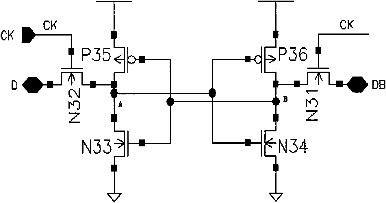
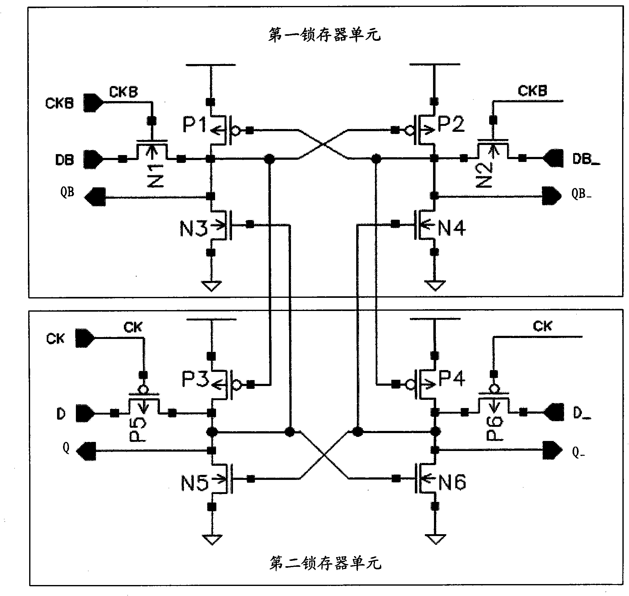
[0015] In the embodiment of the present invention, under common process conditions, redundant storage nodes are introduced into the latch, and when a node is flipped, the voltage of the node can be recovered from other nodes through feedback.

[0016] figure 2 A circuit principle using a design-hardened latch provided by the embodiment of the present invention is shown. Please refer to figure 2 , the latch includes a first latch unit and a second latch unit that are cross-coupled, wherein the clock signal of the first latch unit and the clock signal of the second latch unit are opposite to each...


PUM


Abstract

The invention is suitable for the field of semiconductor devices and provides a high-speed low-power consumption latch device capable of resisting SEU (single event upset). The latch comprises a first latch unit and a second latch unit, which are cross-coupled, wherein a clock signal of the first latch unit is opposite to the clock signal of the second latch unit; a data signal of the first latch unit is opposite to the data signal of the second latch unit; when a stored data value at a sensitive point of the first latch unit upsets, the stored data value at the sensitive point of the first latch unit is recovered by the second latch unit through feedback; and when the stored data value at the sensitive point of the second latch unit upsets, the stored data value at the sensitive point of the second latch unit is recovered by the first latch unit through feedback. In the invention, a redundancy storage node is introduced in the high-speed low-power consumption latch device capable of resisting SEU under a common process condition, and when a node upsets, the voltage of the node can be recovered from other nodes through feedback.

Description

technical field [0001] The invention belongs to the field of semiconductor devices, in particular to an anti-single-event flipping high-speed and low-power consumption latch. Background technique [0002] With the rapid development of aerospace technology, more and more semiconductor devices are used in electronic control systems in the aerospace field. In outer space, there are cosmic rays composed of various rays and single heavy ions. These cosmic rays can cause damage to the electronic control system composed of conventional semiconductor devices. The damage renders it ineffective or even crashes. As the basic instruction storage device of these electronic control systems, its anti-radiation ability is particularly important. Because once the data in the device is wrong, it will directly lead to the failure of the entire system. figure 1 It is an unreinforced latch circuit diagram, in which the size of PMOS transistor P35 and PMOS transistor P36 is smaller than that o...

Claims


Application Information

Patent Timeline
Patent Type & Authority Applications(China)
IPC IPC(8): H03K19/094
Inventor 彭锦军裴国旭徐建强李晓辉罗春华李洛宇
Owner SHENZHEN STATE MICROELECTRONICS CO LTD
Why Eureka
Try Eureka