Ultra-low voltage nand gate circuit

A NOT gate circuit, ultra-low voltage technology, applied in the field of ultra-low voltage NAND gate circuit, to achieve the effect of simple structure, easy design and good symmetry

Inactive Publication Date: 2011-07-20
TSINGHUA UNIV
View PDF3 Cites 1 Cited by
  • Summary
  • Abstract
  • Description
  • Claims
  • Application Information

AI Technical Summary

Problems solved by technology

However, the disadvantage of this NAND gate is that it can be used in ultra-low voltage circuit systems to achieve low power consumption due to the existence of three transistor stack connections.

Method used


Image

  • Ultra-low voltage nand gate circuit
  • Ultra-low voltage nand gate circuit
  • Ultra-low voltage nand gate circuit

Examples


Embodiment Construction

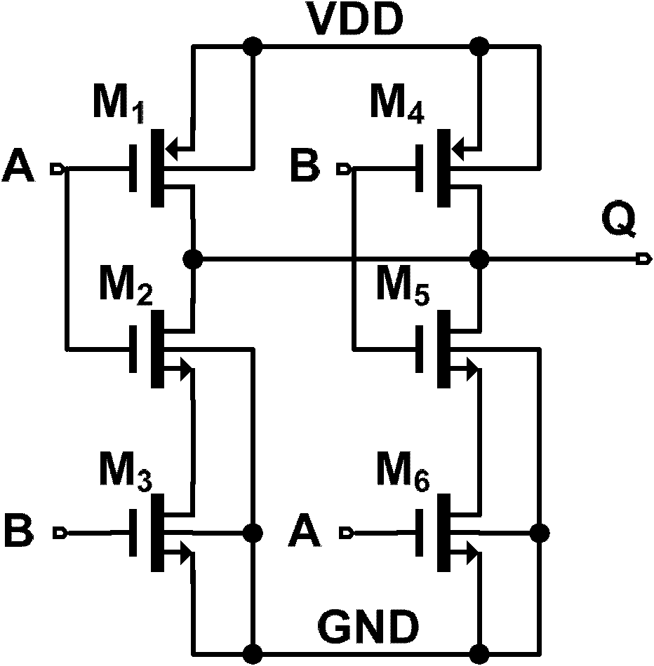
[0025] The ultra-low voltage NAND gate circuit of the present invention is described in detail in conjunction with the drawings and embodiments as follows:

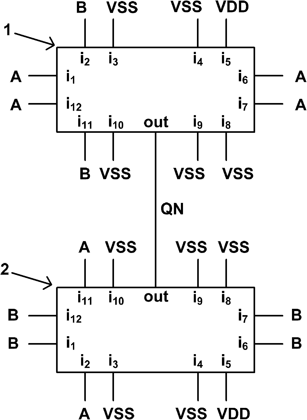
[0026] An ultra-low voltage NAND gate circuit proposed by the present invention, such as figure 2 As shown, it is characterized in that a single-ended input single-ended output structure is adopted, which is composed of a first ultra-low voltage NAND gate basic unit 1 and a second ultra-low voltage NAND gate basic unit 2; The first input terminal i of unit 1 1 Connect to input A, second input i 2 Connect to input B, the third input i 3 Ground voltage VSS, the fourth input terminal i 4 Ground voltage VSS, fifth input terminal i 5 Connect to the power supply voltage VDD, the sixth input terminal i 6 Connect to input A, the seventh input i 7 Connect to input A, the eighth input i 8 Ground voltage VSS, ninth input terminal i 9 Ground voltage VSS, tenth input terminal i 10 Ground voltage VSS, the eleventh input terminal i 11 Conne...


PUM


Abstract

The invention relates to an ultra-low voltage nand gate circuit, which belongs to the field of design of ultra-low voltage circuits implemented by adopting the CMOS (complementary metal oxide semiconductor) process. A single-end input and single-end output structure is constituted by two ultra-low voltage nand gate basic units; and the output ends of the first and the second ultra-low voltage basic units are connected together as the output end of the single-end input and single-end output structure of the ultra-low voltage nand gate circuit. Or a differential input and differential output structure is constituted by four ultra-low voltage nand gate basic units; the input ends of the second and the third ultra-low voltage nand gate basic units are connected as the two differential input ends of the circuit; the input ends of the first and the fourth ultra-low voltage nand gate basic units are connected as the two differential input ends of the circuit; and the output ends of all the basic units are used as the two differential output ends of the circuit respectively. The body biasing technology of a PMOS (positive-channel metal oxide semiconductor) transistor is adopted, thereby being capable of working under ultra-low voltage, being symmetrical and simple in structure, being easy to design, and being good in symmetry of rising edge and falling edge of output signals.

Description

Technical field [0001] The invention belongs to the technical field of ultra-low voltage circuits realized by adopting CMOS technology, and particularly relates to an ultra-low voltage NAND circuit. Background technique [0002] Power consumption is becoming an important limiting factor for VLSI systems. At present, the market demand for portable devices is increasing, and there are more and more electronic products that use batteries as power sources. In order to extend battery life, researchers have increasingly urgent requirements for low-power circuits. For fixed circuit applications, the highest operating temperature also requires lower and lower power consumption of the circuit to ensure the stability of the chip and even the system. From the perspective of circuit realization, when the power supply voltage is reduced to ultra-low voltage (under 0.5 to 0.6V), the power consumption will be drastically reduced. At present, some circuit technologies use special processes, su...

Claims


Application Information

Patent Timeline
Patent Type & Authority Applications(China)
IPC IPC(8): H03K19/20
Inventor 陈勇杨佳乐张莉王燕钱鹤
Owner TSINGHUA UNIV
Why Eureka
Try Eureka