Power MOS transistor of asymmetric structure and array thereof

A MOS transistor and power technology, which is applied in the field of power field effect transistor preparation, can solve the problems of large layout area and achieve the effect of reducing the distance

Inactive Publication Date: 2011-08-03
PEKING UNIV
View PDF5 Cites 9 Cited by
  • Summary
  • Abstract
  • Description
  • Claims
  • Application Information

AI Technical Summary

Problems solved by technology

However, because the distance from the source (1) drain (3) contact hole to the gate is limited by the larger one (the distance from the drain metal contact hole to the gate), it will result in a larger layout area

Method used


Image

  • Power MOS transistor of asymmetric structure and array thereof
  • Power MOS transistor of asymmetric structure and array thereof
  • Power MOS transistor of asymmetric structure and array thereof

Examples


Embodiment Construction

[0015] The present invention will be further described below in conjunction with the examples, but the present invention is not limited to the following examples.

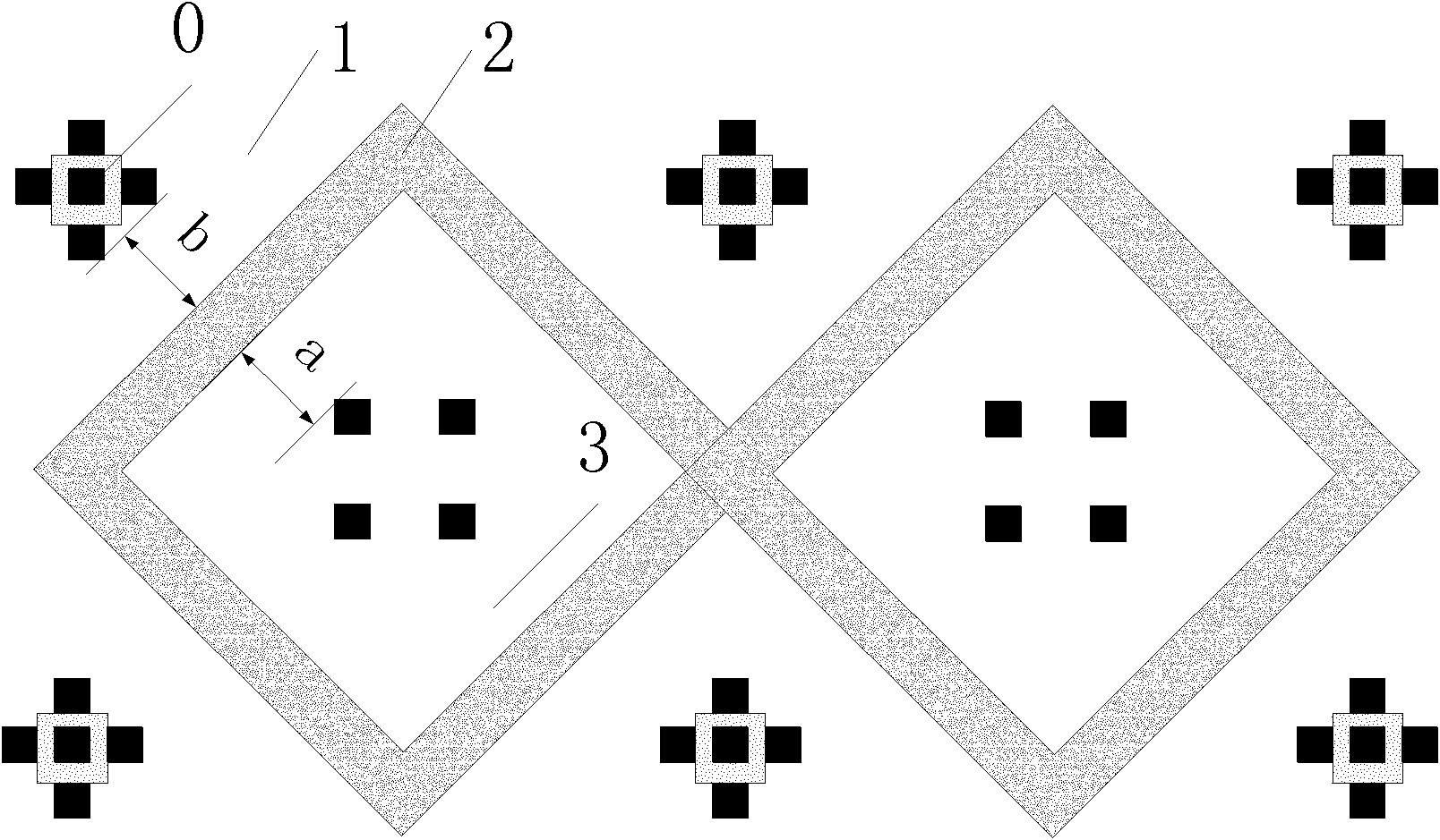
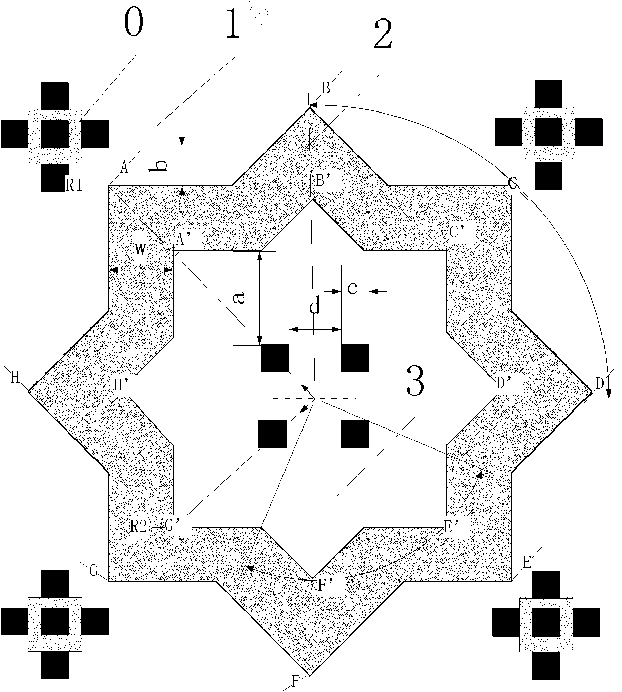
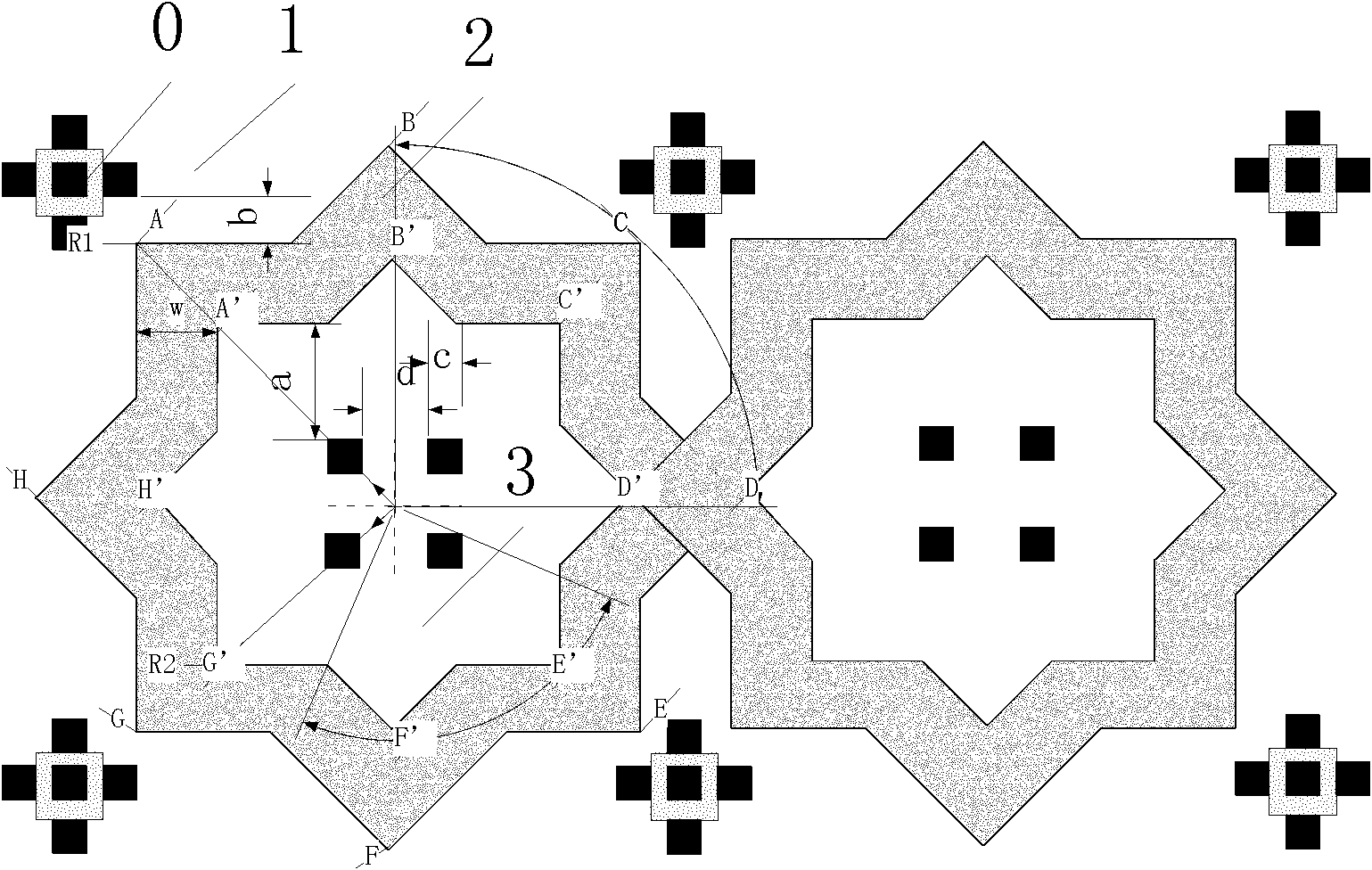
[0016] Take Chartered Semiconductor's 0.35um process as an example. refer to image 3 , Power MOS transistor ESD requirements, the minimum distance from the drain contact hole to the gate structure a=1.7um, the minimum distance from the source contact hole to the gate structure b=0.7um, the width of the gate structure w=0.5um, the drain contact hole The minimum size and minimum pitch is 0.4um.

[0017] Concrete realization of the present invention, by above parameter, with:

[0018] is the radius, and the geometric center of the layout is the center to make a circle. Then do 0 degree, 45 degree, 90 degree, 135 degree straight line and circle intersect to get A, B, C, D, E, F, G and H (135 degree point is A, then marked clockwise), then Respectively connect A, C, E, G and B, D, F, H to form a hexagonal octagon...


PUM


Abstract

The invention provides a power metal oxide semiconductor (MOS) transistor, and belongs to the field of semiconductor devices. The power MOS transistor comprises a source, a drain and a grid structure, wherein the grid structure is specifically designed as: a circle is drawn by using the geometric center of the layout as a circle center, and two sixteen-edge octagonal graphs are made respectively; the edges of the two sixteen-edge octagonal graphs are mutually parallel, a gap between the edges form an octagonal bent belt, and the bent belt is the graph of the grid structure. On the premise of ensuring that the distance between a contact hole of the drain and the grid structure is not changed, the distance between the source and the grid structure is shortened, and smaller layout realization area and lower source connecting metal voltage drop are obtained.

Description

technical field [0001] The invention relates to a preparation technology of a power field effect transistor, which belongs to the field of semiconductor devices. Background technique [0002] At present, the layout of MOSFET transistors used in power management circuits requires the ability to resist ESD (electrostatic discharge). Therefore, in order to be able to withstand large operating current and resist high ESD voltage, traditional power MOSFETs have relatively large source (S) and drain (D) sizes. However, this will inevitably lead to a relatively large layout area. And a larger metal is required to do the interconnection between the drain or the source, which in turn leads to a voltage drop caused by excessive metal resistance. [0003] Traditional power MOS transistors are formed by arranging multiple polysilicon gates at intervals on a substrate. The drain region and the source region are respectively located on two sides of the polysilicon gate on the substrate...

Claims


Application Information

Patent Timeline
Patent Type & Authority Applications(China)
IPC IPC(8): H01L29/78H01L29/423H01L29/08
Inventor 张勇鲁文高黄泽陈博汤耀云陈中建张雅聪吉利久
Owner PEKING UNIV
Why Eureka
Try Eureka