Energy band transmutation multiplication region structure for avalanche photodiode, and preparation method of energy band transmutation multiplication structure

A technology of avalanche photoelectricity and multiplication zone, which is applied in the direction of circuits, electrical components, semiconductor devices, etc., can solve the problem of increasing excess noise, achieve the effect of reducing excess noise and improving the ionization rate difference between electrons and holes

Active Publication Date: 2011-08-17
SHANGHAI INST OF MICROSYSTEM & INFORMATION TECH CHINESE ACAD OF SCI
View PDF4 Cites 19 Cited by
  • Summary
  • Abstract
  • Description
  • Claims
  • Application Information

AI Technical Summary

Problems solved by technology

However, since the superlattice and quantum well structures are alternate barriers and potential wells, to suppress the ionization of one of the electrons or holes without substantially restricting the ionization of the other carrier, it is necessary to add High bias voltage, which will cause the increase of excess noise, the current excess noise parameters are still far from the practical requirements, especially for satellite remote sensing, three-dimensional imaging, high-resolution spectral measurement, single photon detection, etc. In terms of application fields, the requirements for excess noise of devices are higher

Method used


Image

  • Energy band transmutation multiplication region structure for avalanche photodiode, and preparation method of energy band transmutation multiplication structure
  • Energy band transmutation multiplication region structure for avalanche photodiode, and preparation method of energy band transmutation multiplication structure
  • Energy band transmutation multiplication region structure for avalanche photodiode, and preparation method of energy band transmutation multiplication structure

Examples


Embodiment 1

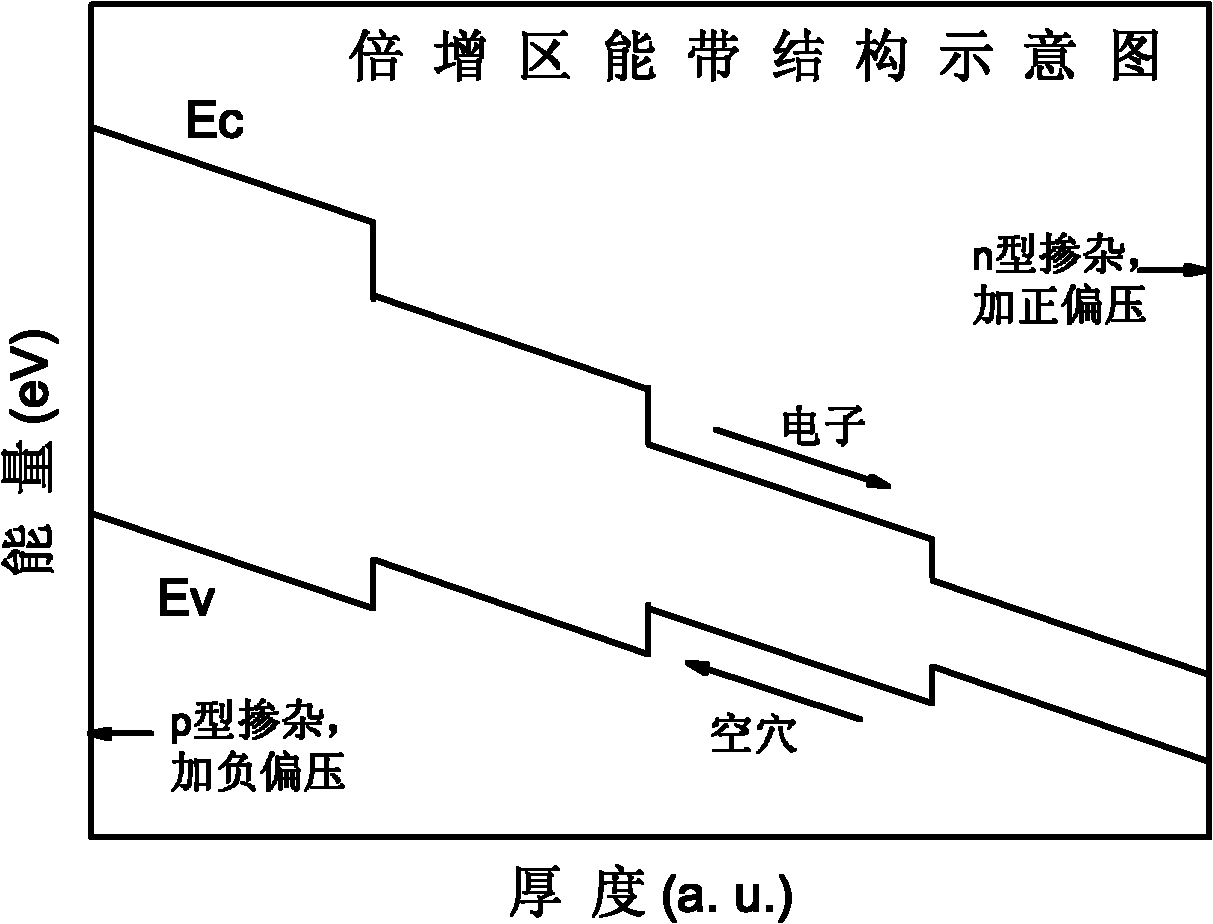
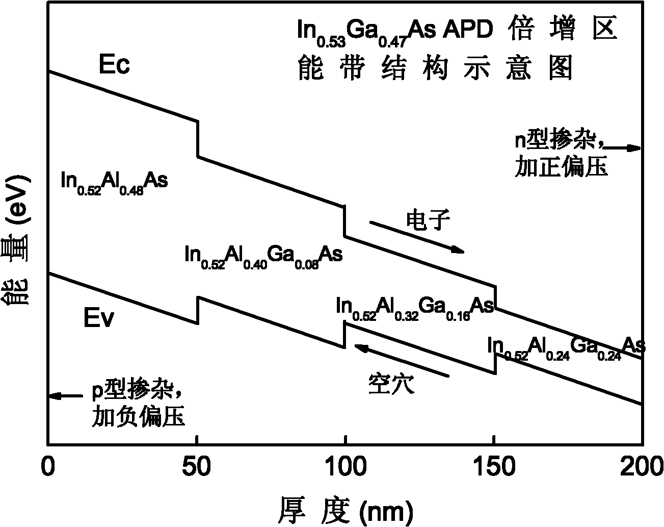
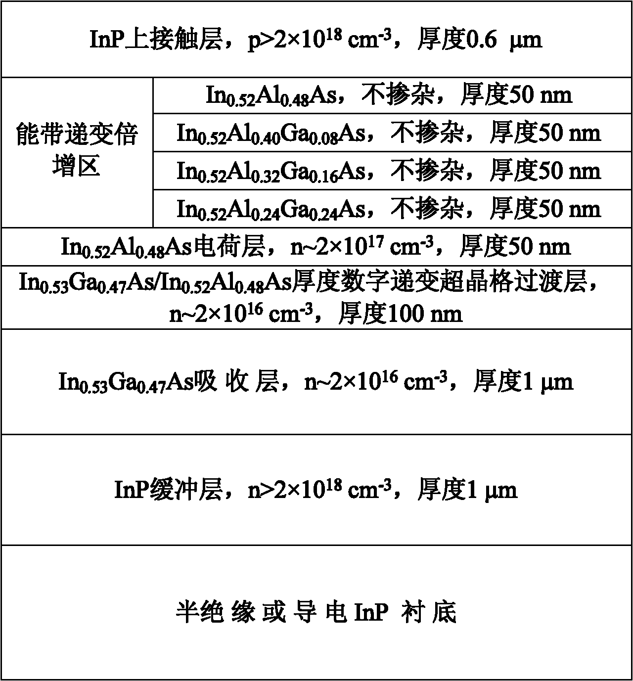
[0029] (1) need to grow In 0.53 Ga 0.47 As avalanche photodiode epitaxial material, the absorption region charge region and the multiplication region are separated, with a transition layer (SAGCM) structure, semi-insulating or conductive InP single crystal material is used as the substrate of the detector, InP material is used as a buffer layer and Si is used for high Doping (at the same time as the lower contact layer, n>2×10 18 cm -3 ), In 0.53 Ga 0.47 The As material is used as the absorber layer for low doping Si or no doping (n~2×10 16 cm -3 ), lower doped Si In 0.52 Al 0.48 As as the charge layer (n~2×10 17 cm -3 ), without doping In 0.53 Ga 0.47 As / In 0.52 Al 0.48 The As superlattice is used as the transition layer between the absorption layer and the charge layer, and the multiplication region uses undoped four layers of In with different compositions. 0.52 Al x Ga 0.48-x The As material constitutes an energy band gradient structure, and the schematic dia...


PUM


Abstract

The invention relates to an energy band transmutation multiplication region structure for an avalanche photodiode, and a preparation method of the energy band transmutation multiplication structure. The invention is characterized in that: an n-layer material of which the energy band gradient is transmuted is used as the multiplication region structure, n is a natural number, and x is more than orequal to 2 and less than or equal to 10. The preparation method comprises a step of: growing the n-layer material of which the energy band gradient is transmuted as a multiplication region structure after growing a buffer layer, an absorption layer, a digital transmutation superlattice transitional layer and a charge layer. By the energy band transmutation multiplication region structure, the ionization rate difference between electrons and cavities can be increased substantially, and external very high bias voltage is not needed; therefore, the over-residual noises of the device can be reduced effectively.

Description

technical field [0001] The invention belongs to the field of avalanche photodiode and its preparation, and in particular relates to a band-gradient multiplication region structure for avalanche photodiode and a preparation method thereof. Background technique [0002] Avalanche Photodiode (APD) has higher sensitivity and detectability than PN detectors due to its multiplication effect, and is especially suitable for the detection of weak light signals, and has gained more and more attention and applications. Since the appearance of APD in the 1970s, the structure of APD has undergone a continuous improvement process. The early APD structure still uses the PIN structure, but it works at a higher reverse voltage, but the higher working voltage makes the device have a lot of excess noise. In order to reduce device noise, the researchers designed a structure that separates the absorption region and the gain region, and added a multiplication region with a relatively wider band ...

Claims


Application Information

Patent Timeline
Patent Type & Authority Applications(China)
IPC IPC(8): H01L31/107H01L31/0352H01L31/18
Inventor 顾溢张永刚
Owner SHANGHAI INST OF MICROSYSTEM & INFORMATION TECH CHINESE ACAD OF SCI
Why Eureka
Try Eureka