Element mounting device and element mounting method

A technology of installation device and installation position, which is applied in the direction of assembling printed circuits, electrical components, electrical components, etc. with electrical components, and can solve problems such as poor welding

Active Publication Date: 2011-08-24
YAMAHA MOTOR CO LTD
View PDF4 Cites 28 Cited by
  • Summary
  • Abstract
  • Description
  • Claims
  • Application Information

AI Technical Summary

Problems solved by technology

Therefore, as will be described later, the solder protruding from the electrodes melts and adheres to the end faces of the el

Method used


Image

  • Element mounting device and element mounting method
  • Element mounting device and element mounting method
  • Element mounting device and element mounting method

Examples


Embodiment approach

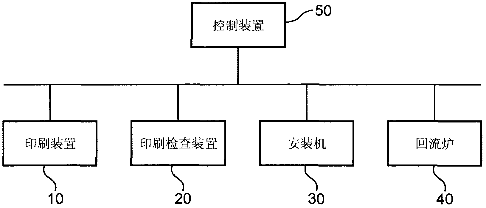
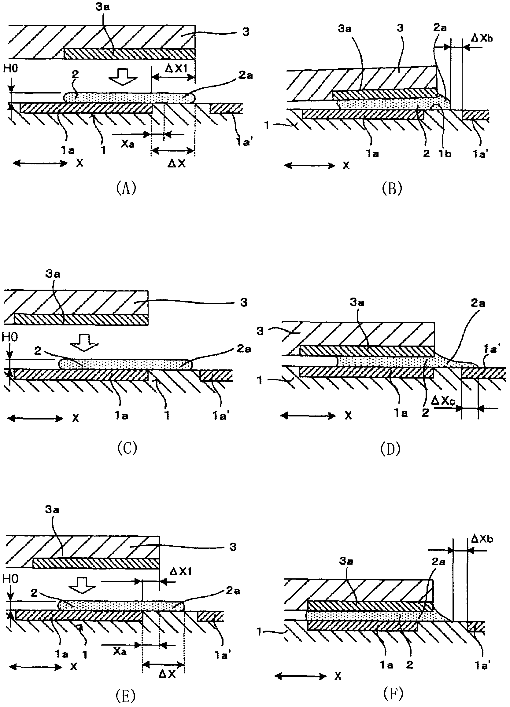
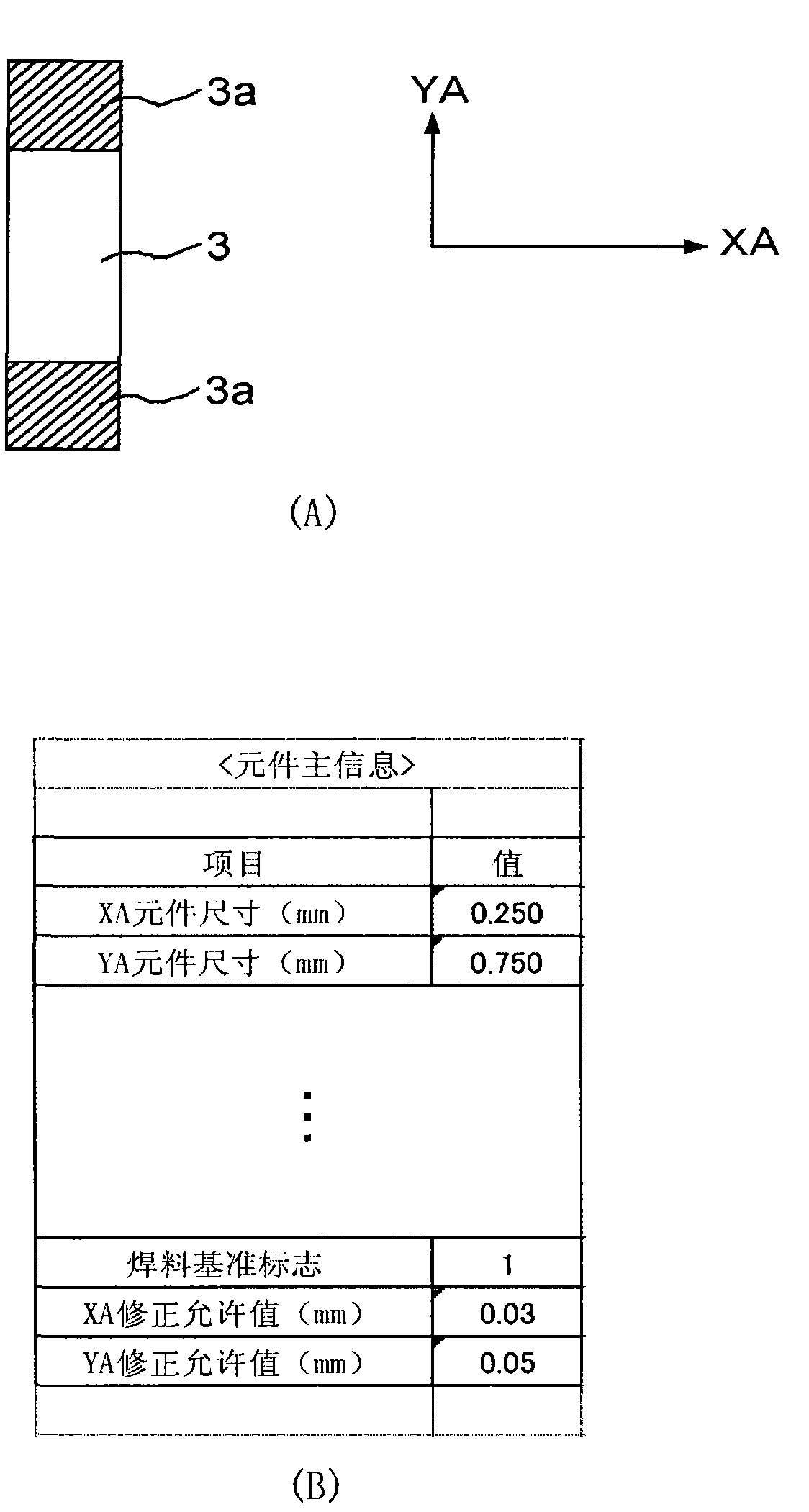
[0040] Figure 5 It is a plan view which shows the mounting machine which is one embodiment of the component mounting apparatus concerning this invention. Figure 6 yes means Figure 5 Block diagram of the main electrical structure of the setup machine shown. In this mounter 30 , a board transfer mechanism 302 is provided on a base 311 to transfer the printed board 1 on which cream solder has been printed by the printing device 10 in a predetermined transfer direction (+X axis direction). More specifically, the substrate transfer mechanism 302 has the function of transferring the substrate 1 from the base 311 to Figure 5 A pair of conveyor belts 321, 321 are conveyed to the left side from the right side. After the conveyor belts 321, 321 carry in the substrate 1, they are stopped at a designated mounting operation position (the position of the substrate 1 shown in this figure), and the substrate 1 is fixed and held by a holding device not shown in the figure. Next, the el...


PUM


Abstract

The invention provides an element mounting device and an element mounting method. The element mounting device comprises a head assembly and a control part. Elements are installed on a substrate by the head assembly. The motion of the head assembly is controlled by the control part. Meanwhile, the mounting position of elements is adjusted according to the printing offset of the solder with respect to the electrode. When the printing offset is within a correction permissible range, the elements are installed on the substrate with the offset position of the solder on the substrate as a reference. The correction permissible range is set according to the self-correction effect exhibited by the fused solder, so that the mounting position of the elements is corrected to be at the electrode side. When the printing offset exceeds the correction permissible range, the elements are installed with the specified position close to the electrode as a reference within the offset range of the solder on the substrate. Therefore, the mounting position of the elements is adjusted according to the offset, so that the bad welding is prevented and the elements are satisfactorily installed on the substrate.

Description

technical field [0001] The present invention relates to a component mounting device and a component mounting method for mounting components on a substrate on which solder is printed on electrodes. Background technique [0002] In order to manufacture a substrate on which electronic components are mounted (hereinafter referred to as "component mounting substrate"), the following steps are sequentially performed: Printing solder on electrodes formed on the substrate, so-called substrate electrodes (or pads), by a printing device A printing process; a mounting process of mounting components on a substrate printed with solder by a component mounting device; a reflow process of passing a substrate mounted with components through a reflow furnace. In the printing process among these steps, paste-like solder is printed on the surface of the substrate through the openings of the stencil while the stencil formed with the openings corresponding to the substrate electrode patterns is a...

Claims


Application Information

Patent Timeline
IPC IPC(8): H05K13/04H05K3/34
CPCH05K13/0408H05K13/0413H05K13/0465
Inventor 中川义之三宅祥史
Owner YAMAHA MOTOR CO LTD
Why Eureka
Try Eureka