Automatic control method and device of PCB layout

An automatic control device and layout technology, applied in the direction of printed circuit manufacturing, multilayer circuit manufacturing, electrical components, etc., can solve the problems of error-prone, cost-prone, manual omission, etc., and achieve the effect of avoiding poor tinning

Active Publication Date: 2019-04-09
ZHENGZHOU YUNHAI INFORMATION TECH CO LTD
View PDF4 Cites 1 Cited by
  • Summary
  • Abstract
  • Description
  • Claims
  • Application Information

AI Technical Summary

Problems solved by technology

Since there are many soldering parts in the DIP package on the server board, if the layout engineer manually handles the number of connection layers of the PTH hole, it will take a lot of time, and i

Method used


Image

  • Automatic control method and device of PCB layout
  • Automatic control method and device of PCB layout
  • Automatic control method and device of PCB layout

Examples


Embodiment 1

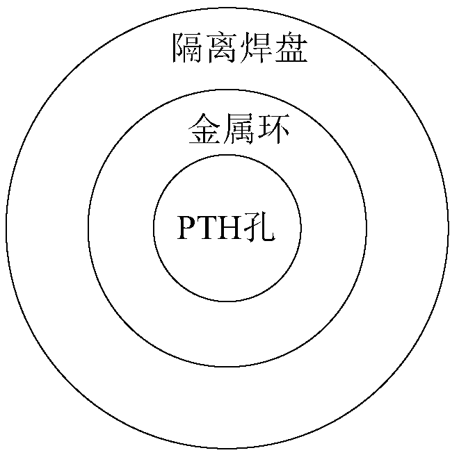
[0050] When using the allegro software developed by Cadence for PCB design, through the secondary development skill of the candence software, the number of connection layers of the PTH holes is limited. Once more than 3 layers are connected, the copper surface will be laid on the back and it will automatically follow the PTH. The antipad size of the hole is avoided. Specifically, when using the allegro software developed by Cadence for PCB design, by writing a skill program that limits the number of PTH hole connection layers and automatically avoids the copper surface of the same attribute according to the size of the antipad after the number of layers exceeds the limit, then the Skill program Put it into the Skill menu, and execute the Skill program to set the requirements for the number of connection layers for all PTH holes, and automatically avoid the problem of too many connection layers for PTH holes during layout design.

[0051] The specific steps can be as follows: ...

Embodiment 2

[0059] The automatic control method of the PCB layout of the embodiment of the present invention, comprises the steps:

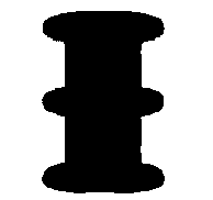
[0060] 1. If image 3 As shown, set the power pins of the slot, such as three 3v3 PTH holes on the left and four 12V PTH holes on the right.

[0061] 2. Run the skill program and the following dialog box will appear. Such as Figure 4 Shown:

[0062] 3. Select the PTH hole to be set to image 3 Take the 7 PTH holes as an example, select them and click OK.

[0063] 4. After the setting is completed, output the done command.

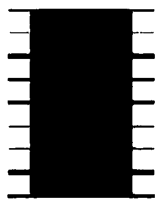
[0064] 5. When the fourth layer of copper surface is laid, it will automatically avoid the connection according to the antipad size of the PTH hole (take 12v as an example). Its effect is as Figure 5 shown.

[0065] image 3 and Figure 5 Among them, the black area covering 3V3 is the conductive copper skin of 3V3 property, and the black area covering 12v is the copper skin of 12v property, that is, the conductive copper skin ...


PUM


Abstract

The invention discloses an automatic control method and device of printed circuit board PCB layout. The method comprises the following steps: in the PCB layout process, when a new conducting layer isincreased, for a predetermined PTH hole, judging whether the amount of conducting layer currently connected by a PTH hole has reached the preset maximum amount of layer, if the amount of conducting layer currently connected by a PTH hole has reached the preset maximum amount of layer, electrically isolating the PTH hole from the newly added conducting layer. Through the scheme disclosed by the invention, the amount of connecting layer of the PTH hole can be accurately and efficiently restricted, thereby avoiding the problem that the tinning is bad due to overmuch amount of connecting layer ofthe PTH hole.

Description

technical field [0001] The present invention relates to the automatic control technology of PCB layout, especially a kind of automatic control method of PCB layout. Background technique [0002] With the rapid development of server products and the mass production of server PCB boards, how to quickly improve design and production efficiency and the pass rate of PCB boards has become a key factor in determining time costs and material costs. [0003] In one of the upper parts of PCB board production, that is, PCBA (Printed Circuit Board + Assembly) production, many DIP (dual inline-pin package, dual inline-pin package technology, also known as dual internal line packaging or hand plug-in There is a problem of poor tinning on the soldered parts of the package. After the production of the board is completed, another tin filling treatment is required to make the parts welded firmly and ensure the continuous stability of the product. [0004] After analysis, it was found that t...

Claims


Application Information

Patent Timeline
IPC IPC(8): H05K3/42H05K3/46H05K3/00H05K1/11
CPCH05K1/115H05K3/0005H05K3/429H05K3/4679
Inventor 王英娜
Owner ZHENGZHOU YUNHAI INFORMATION TECH CO LTD
Why Eureka
Try Eureka