Surface mount structure and circuit board with same

A surface mount and circuit board technology, applied in the direction of printed circuits connected with non-printed electrical components, printed circuit components, electrical connection printed components, etc., can solve problems affecting the quality of electronic component placement, and improve signal quality The effect of transmitting quality, avoiding poor welding, and improving placement quality

Active Publication Date: 2012-07-04
AVARY HLDG (SHENZHEN) CO LTD +1
View PDF0 Cites 0 Cited by
  • Summary
  • Abstract
  • Description
  • Claims
  • Application Information

AI Technical Summary

Problems solved by technology

However, when the distance between a pad with a small surface area and a pad with a large surface area is short, that is, when the connection line is short (for example, less than 0.3mm), when the solder resist cannot be coated or printed, the above remelting The problem of solder flowing from pads with a smaller surface area to pads with a larger surface area still exists, which seriously affects the placement quality of electronic components

Method used


Image

  • Surface mount structure and circuit board with same
  • Surface mount structure and circuit board with same
  • Surface mount structure and circuit board with same

Examples


Embodiment Construction

[0018] The surface mount structure of the technical solution and the circuit board with the surface mount structure will be described in further detail below with reference to the drawings and embodiments.

[0019] The embodiment of the technical solution provides a surface mount structure, which is used for fixedly mounting electronic components with pins and solder chassis on a circuit board.

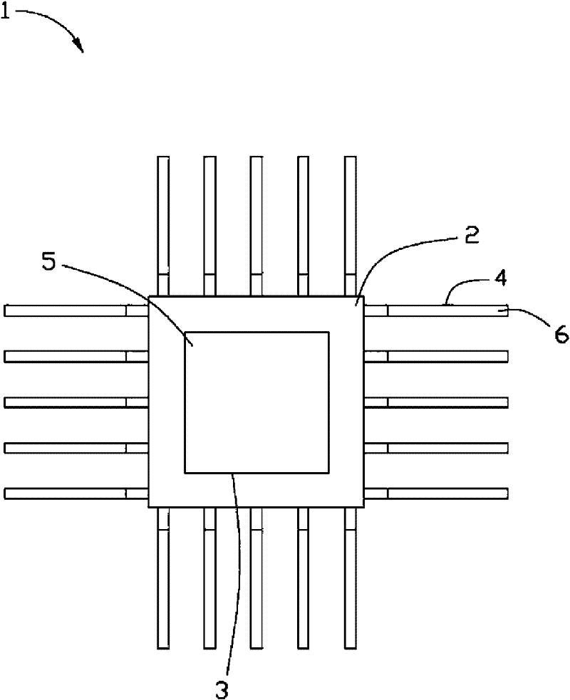
[0020] See figure 1 The above-mentioned electronic component 1 for mounting has a chip main body 2, a soldering chassis 3, and pins 4. Among them, the welding chassis 3 is formed on the bottom surface of the chip main body 2, and the pins 4 are formed on the peripheral edges of the chip main body 2. The welding chassis 3 has a first bottom surface 5 for welding. The pin 4 has a second bottom surface 6 for soldering.

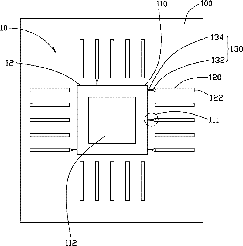
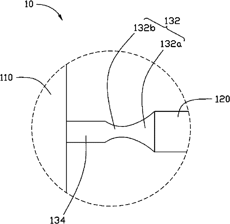
[0021] See figure 2 versus image 3 In the first embodiment, the surface mount structure 10 includes pads 12 formed on the circuit board 100. Wherein, the pad 12 includes a...


PUM


Abstract

The invention provides a surface mount structure used for fixedly mounting an electronic element with a pin and a welding chassis onto a circuit board. The surface mount structure comprises a pad formed on the circuit board, wherein the pad comprises a first pad welded with the bottom surface of the pin, a second pad welded with the bottom surface of the welding chassis and a connecting wire for connecting the first pad and the second pad. The structure is characterized in that the area of the surface of the second pad, which is opposite to the bottom surface of the welding chassis, is largerthan the area of the surface of the first pad, which is opposite to the bottom surface of the pin; the space between the first pad and the second pad is smaller than 0.3mm; the connecting wire comprises a current-limiting part and a non-current-limiting part; the current-limiting part is connected with the first pad, and the non-current-limiting part is connected with the second pad; and the partial or overall wire width of the current-limiting part is smaller than the wire width of the non-current-limiting part.

Description

Technical field [0001] The present invention relates to circuit board technology, in particular to a surface mount structure that can be used for mounting electronic components and a circuit board with the surface mount structure. Background technique [0002] With the rapid development of the electronics industry, the manufacturing technology of circuit boards, which are the basic components of electronic products, is becoming more and more important. Circuit boards are generally made of copper-clad substrates through a series of processes such as cutting, drilling, etching, exposure, development, pressing, and molding. For details, please refer to the article "Dielectric characterization of printed circuit board substrates" published by C.H. Steer et al. in Proceedings of the IEEE, Vol. 39, No. 2 (August 2002). [0003] Generally, after the circuit board is manufactured, various electronic components need to be mounted on the circuit board. Therefore, the surface of the circuit...

Claims


Application Information

Patent Timeline
Patent Type & Authority Patents(China)
IPC IPC(8): H05K1/11H05K1/18
Inventor 邹立
Owner AVARY HLDG (SHENZHEN) CO LTD
Why Eureka
Try Eureka