Method for grinding indium antimonide wafer

An indium antimonide wafer and indium antimonide technology are applied in grinding/polishing equipment, grinding/polishing safety devices, and machine tools suitable for grinding workpiece planes, etc. Inefficiency and other problems, to achieve the effect of reducing edge collapse, improving yield, and improving consistency

Active Publication Date: 2011-09-07
11TH RES INST OF CHINA ELECTRONICS TECH GROUP CORP
View PDF5 Cites 8 Cited by
  • Summary
  • Abstract
  • Description
  • Claims
  • Application Information

AI Technical Summary

Problems solved by technology

[0006] The invention provides a grinding method for indium antimonide wafers, which is used to solve the problems of poor consist

Method used


Image

  • Method for grinding indium antimonide wafer
  • Method for grinding indium antimonide wafer

Examples


Embodiment Construction

[0021] The present invention will be described in further detail below in conjunction with the accompanying drawings and embodiments. It should be understood that the specific embodiments described here are only used to explain the present invention, not to limit the present invention.

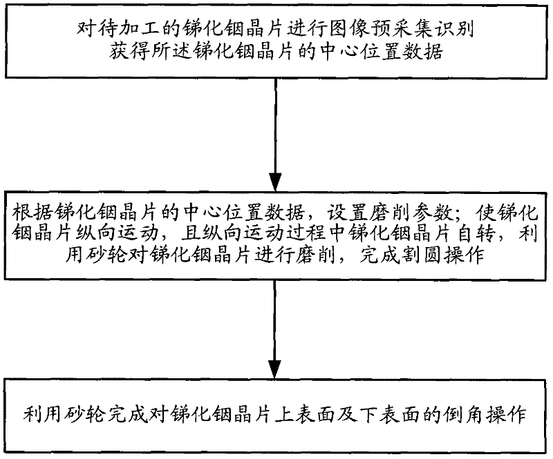
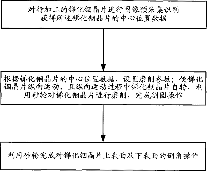
[0022] In order to solve the problem of circle cutting and chamfering process of 3-inch indium antimonide wafer, the present invention provides a wafer shape recognition based on wafer image recognition technology and matching process of cutting circle and chamfering indium antimonide wafer, which not only solves the problem of It solves the problems of accuracy, poor consistency, and high labor intensity of the existing manual processing technology, and effectively solves the problem of batch and large-scale production of indium antimonide wafers, and provides a method for dividing the plane into circles and concaves in multiple steps after wafer identification. The subsequent treatment proce...


PUM


Abstract

The invention discloses a method for grinding an indium antimonide wafer. The method comprises the following steps of: performing image pre-acquisition and identification on the indium antimonide wafer to be processed to acquire central position data of the indium antimonide wafer; setting grinding parameters according to the central position data of the indium antimonide wafer; making the indium antimonide wafer move longitudinally and rotate during longitudinal movement, and grinding the indium antimonide wafer by using a grinding wheel to finish circle cutting operation; and finishing chamfering operation on the upper surface and the lower surface of the indium antimonide wafer by using the grinding wheel. By the method, the positions of the center and the reference surface of the wafer are accurately positioned, and circle cutting treatment and chamfering treatment are performed during grinding after wafer identification to achieve the multi-step and accurate grinding effects. Edge breakage in the chamfering process is effectively reduced, repeatability of process conditions is ensured, the consistency of wafer appearance is improved, and the yield is improved.

Description

technical field [0001] The invention relates to the technical field of semiconductors, in particular to a grinding method of an indium antimonide wafer. Background technique [0002] One of the remarkable advantages of infrared focal plane detection technology is that it can obtain more ground target information, and has broad application prospects in target search, missile early warning detection, intelligence reconnaissance and other military and related civilian fields. In order to meet the large-scale development of the area array of indium antimonide focal plane array devices, it is necessary to develop 3-inch indium antimonide wafer materials. [0003] The shape standardization process of 3-inch indium antimonide wafer is one of the key processes of indium antimonide wafer processing technology. Due to the particularity of the indium antimonide material itself, the wafers processed by crystals grown in the <111> direction have poor consistency in electrical para...

Claims


Application Information

Patent Timeline
IPC IPC(8): B24B7/22B24B9/06B24B55/02H01L21/304
Inventor 王志芳王燕华程波陈元瑞程鹏王森林
Owner 11TH RES INST OF CHINA ELECTRONICS TECH GROUP CORP
Why Eureka
Try Eureka