Basic input/output system (bios) and interrupt realizing method for Loongson central processing unit (CPU) mainboard

A technology of Godson and mainboard, applied in the field of mainboard bios and interrupt realization, which can solve problems such as interrupt distribution and achieve the effect of ensuring normal operation

Active Publication Date: 2011-09-14
中科可控信息产业有限公司
2 Cites 24 Cited by

AI-Extracted Technical Summary

Problems solved by technology

[0010] In order to obtain a bios and linux kernel that can run on the Loongson motherboard, and solve the problems of address mapping, PCI configuration s...

Abstract

The invention provides a basic input/output system (bios) realizing method for a Loongson central processing unit (CPU) mainboard. The method comprises the following steps of: performing address mapping conversion on the Loongson CPU and a north bridge chip; performing mapping conversion on the addresses of direct memory access (DMA) equipment; configuring peripheral command indicator (PCI) address space; debugging after fusing a coreboot and a process monitor (pmon) into a new bios; and debugging a kernel interrupt system. By the method provided by the invention, the problem of address mapping conversion between the Loongson CPU and advanced micro device (AMD) bridge piece on a BIOS layer, the problem of DMA equipment addressing in the PMON, the problem of reading and writing in PCI configuration space of a Loongson blade and the problems of transplanting and debugging from the coreboot to the pmon are solved. Moreover, the interrupt processing mode of the external equipment of the Loongson mainboard ensures the normal operation of the external equipment on the Loongson mainboard.

Application Domain

Multiprogramming arrangements

Technology Topic

Embedded systemAddress space +10

Image

  • Basic input/output system (bios) and interrupt realizing method for Loongson central processing unit (CPU) mainboard
  • Basic input/output system (bios) and interrupt realizing method for Loongson central processing unit (CPU) mainboard
  • Basic input/output system (bios) and interrupt realizing method for Loongson central processing unit (CPU) mainboard

Examples

  • Experimental program(1)

Example Embodiment

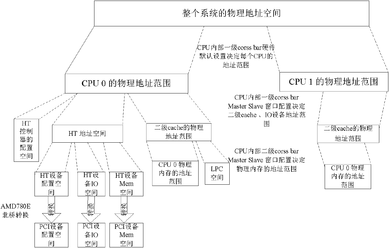
[0040] 1. Conversion of Loongson CPU and North Bridge address mapping
[0041] In the x86 platform, the address of the system is divided into physical address, bus address and virtual address. In Linux, the 4GB (virtual) memory of a process is divided into user space and kernel space. The user space is distributed as 0~3GB (ie PAGE_OFFSET, which is equal to 0xC0000000 in 0X86), and the remaining 1G is the kernel space. Programmers can only use virtual addresses. Each process in the system has its own private user space (0-3G), which is invisible to other processes in the system. The address when the CPU issues an instruction fetch request is the virtual address of the current context, and the MMU finds the physical address of this virtual address from the page table to complete the instruction fetch. And the x86 platform uses a technology called memory mapping (MMIO), which is part of the PCI specification. The IO device port is mapped to the memory space. After mapping, the CPU accesses the IO port as if it were accessing memory. figure 2 It is the MEM mapping address of several devices of AMD bridge chips in coreboot, and 'h' represents hexadecimal.
[0042] The Loongson CPU is a MIPS architecture CPU, which differs from the x86 CPU in address allocation and addressing. Loongson 3A uses a 48-bit physical address space, 47-44 bits distinguish 16 nodes, and 44-0 is the internal address of each node; Loongson blade server is a CC-NUMA architecture composed of two nodes. The address space can be divided into four levels, namely the physical address range, the address space of the first and second level crossbar routes in the node, the address space of the HT, and the address space of the PCI. The next level is a subinterval of the previous level, see image 3 shown.
[0043] There must be a master node with a node_id of 0 in the system, which is responsible for the startup of the system. The node_id of another node of the Loongson blade server is set to 01 by a hardware jumper, so the physical address space of the entire system ranges from [0x0000_0000_0000 to 0x2000_0000_0000], where [ 0x0000_0000_0000~0x1000_0000_0000] is the physical address range of node 0, and [0x1000_0000_0000~0x2000_0000_0000] is the physical address range of node 01.
[0044] The devices connected to the north and south bridge chips are all PCI devices. The PCI system has 4GB of memory space and 64K of IO space. To access the configuration space, memory space, and IO space of the PCI device, the CPU needs to go through a series of conversion processes, that is, 48-bit CPU address space → 40-bit HT address space → PCI address space. like Figure 4 shown.
[0045] 1. Conversion from the physical address space of the CPU to the HT address space
[0046] Loongson 3A maps the CPU physical address space [0x0e00_0000_0000~0x1000_0000_0000] to the 40-bit address space of HT [0x00_0000_0000~0x100_0000_0000]. This mapping is realized through the address routing window of the first-level crossbar or the default settings of the first-level crossbar. Because the HT has only 40 bits of address space, the extra bits are not considered.
[0047] 2. Conversion of HT address space to PCI address space
[0048]The mapping from the HT 40-bit address space to the PCI address space is implemented through the HT to PCI bridge, which is guaranteed by hardware and does not require any configuration by software. After mapping, the starting MEM address of the PCI device is 0x10000000, and the starting address of IO is 0x18000000. This address is used as the MEM BASE or IO BASE of PCI in the PMON program. For each PCI device, PMON creates a pci_device structure. In this structure, the information of each PCI device is recorded, including the type of the device, the size of mem, and the pointer of the next device, etc., forming a linked list. During the PCI device scanning process, PMON will recursively search for resource request information of all devices according to the linked list, and form a pci_win structure to form a memory and IO resource request linked list. In the process of PCI device resource allocation, memory and IO are allocated according to the following formula:
[0049] PCI device MEM address = MEM address of the previous device + MEM request size of the PCI device
[0050] PCI device IO address = MEM address of the previous device + IO request size of the PCI device
[0051] The initial value of the MEM address of the first device is equal to 0x10000000, and the IO address is 0x18000000. In the PMON program, the MEM and IO sizes of the device are obtained by reading the configuration space of the PCI device, thereby allocating the MEM and IO addresses of the PCI device.
[0052] Second, the device DMA operation configuration on the Loongson 3A motherboard:
[0053] In the Loongson CPU, the device accesses the memory by DMA as follows:
[0054] 1. The memory access address sent by the PCI device passes through the north bridge chip, and is routed from the north bridge to the HT1 controller;
[0055] 2. The HT1 controller routes the address to the first-level crossbar according to its internal address window register
[0056] 3. The first-level crossbar routes the address to the second-level cache according to its internal address window register, and then to the second-level crossbar;
[0057] 4. The secondary crossbar routes addresses to the memory controller according to its internal address window configuration.
[0058] The north and south bridge chips are connected to many devices that need to perform DMA operations, such as network card devices, which need to perform DMA operations when receiving and sending data packets. Because of the difference in the physical address of the memory between the X86 architecture and the MIPS architecture, it is necessary to modify the settings of the relevant DMA operation registers of the north bridge in the BIOS, otherwise the DMA operation will not be performed correctly. In the present invention, the relevant registers of the north bridge are modified as follows in the PMON: the value of nbconfig 0x90 is changed from 0x40000000 to 0xf0000000, thereby ensuring that the DMA operation addresses of the north and south bridge equipment are correct and the normal operation of the equipment DMA.
[0059] 3. Loongson blade PCI configuration space and IO space read and write:
[0060] The initialization code of the north-south bridge device in the Loongson blade BIOS mainly draws on the BIOScoreboot of the x86 architecture. In coreboot, the north-south bridge chip initialization code is completely implemented according to the working principle of X86 CPU. The Godson 3 processor is a MIPS architecture CPU, which is completely different from the X86 architecture in terms of address space, PCI configuration space read and write access, etc., which requires us to rewrite the initialization code of the north and south bridge chips, mainly for the north and south bridge devices PCI Modification of the read and write functions of the configuration space, etc.
[0061] The BIOS programs used by the X86 architecture CPU basically use the PCI-compatible configuration method to read and write the PCI configuration space registers.
[0062] The PCI-compatible configuration method uses two 32-bit IO ports, namely the configuration address port 0xCF8 and the configuration data port 0XCFC. Configure the address port data format such as Figure 5 shown.
[0063] When you want to read the contents of the PCI configuration space register of the device, you need to write the bus number, device number, function number, register location and other information of the device to the configuration address port, and then read the configuration data port, you can get the PCI configuration space related registers. content.
[0064] When you want to write the content of the PCI configuration space register of the device, you need to write the bus number, device number, function number, register location and other information of the device to the configuration address port, and then write the data to the configuration data port, you can write the relevant content. to the PCI configuration space related registers.
[0065] PCI, PCI-E bus can use this method to read and write the PCI configuration space register inside the device on the bus. Using this method, 8-bit, 16-bit, and 32-bit read and write operations can be directly performed on the PCI configuration space registers.
[0066] Under the MIPS architecture, the HT bus configuration method is used to read and write the PCI configuration space register.
[0067] The HT bus configuration method means that the HT bus can use the PCI-compatible configuration method to read and write the PCI configuration space registers inside the device on the bus, or use its own unique configuration method to perform operations on the PCI configuration space registers inside the device on the bus. Read and write operations.
[0068] Under the MIPS architecture, the address format of type 0 and type 1 is as follows Image 6 As shown, the 40-bit to 63-bit address needs to be determined according to the CPU and the HT bus, and the address we use at present is 0x90000E. On the Loongson 3A motherboard, we define the type 0 address HT_MAP_TYPE0_CONF_ADDR as 0xba000000, and the type 1 address HT_MAP_TYPE1_CONF_ADDR as 0xbb000000.
[0069] When you want to read the contents of the PCI configuration space register of the device, you need to add the bus number, device number, function number, register location and other information of the device to the first address to get the final read and write access address. The formula is as follows:
[0070] addr|=(dev<<11|func<<8|reg)
[0071] where addr=HT_MAP_TYPE0_CONF_ADDR or
[0072] HT_MAP_TYPE1_CONF_ADDR; reg is the PCI register number that needs to be operated.
[0073] When the last obtained address is read and accessed, the contents of the relevant registers of the PCI configuration space can be obtained; when the relevant data is written to the last obtained address, the relevant contents can be written to the relevant registers of the PCI configuration space.
[0074] For IO operations, under the X86 architecture, there is an IO address space ranging from 0x0-0xffff, which can be accessed using the in and out instructions. In the MIPS architecture, there is no direct corresponding IO address space, and there is no direct corresponding to in and out instructions to access the IO address space. However, some devices such as serial ports, real-time clocks, interrupt controllers, and IDEs need to perform corresponding read and write operations on the IO address space they use when they are working normally. In this way, under the MIPS architecture, corresponding read and write operations must be implemented to make these devices work normally. To solve this problem, use 0xFDFC000000 in the HT address window as the IO address space. The mapped base address of this area is 0xb8000000. The formula for this IO address is:
[0075] addr|=BONITO_PCIIO_BASE_VA+addr
[0076] Where BONITO_PCIIO_BASE_VA=0xb8000000
[0077] Therefore, in order to achieve seamless migration from coreboot to pmon, it is necessary to modify and add the read and write functions of the PCI configuration space and the read and write functions of the IO space. Changed and added function interfaces include 8-bit, 16-bit, 32-bit read operation functions of PCI configuration space registers; 8-bit, 16-bit, 32-bit write operation functions of PCI configuration space registers; PCI configuration space type 0, type 1 read/write Method; debug information output function; memory register 8-bit, 16-bit, 32-bit read and write functions; IO register 8-bit, 16-bit, 32-bit read and write functions; initialization configuration parameter setting function; device search function; device positioning function etc.; other things that need to be changed include IO address macro definitions, etc.;
[0078] Fourth, the pmon debugging method of the Loongson 3A motherboard
[0079] In the initial stage of the debugging of the Loongson 3A motherboard, there is no guarantee that the code for the initialization of the north and south bridges in pmon is correct, and all devices can work normally. In order to ensure the power-on debugging progress of the Loongson blade motherboard and reduce the complexity of the debugging work, we choose a simplified method, that is, before the PCI device scanning of the pmon code, shield the complex and unused devices in the north and south bridges , and carry out subsequent debugging of necessary equipment.
[0080] Figure 7 Initialize the flowchart for the PMON code:
[0081] It can be seen from the flow chart that PMON mainly debugs the CPU, memory and serial port in the assembly part. After entering the C language part, it starts the initialization of the north and south bridge controllers and devices. In the initialization process of the north and south bridges, the controllers of each device will be enabled and initialized first, so that the devices under the enabled controllers will be enumerated during the PCI scan process, while the unenabled controllers will be Do not enumerate and allocate resources. Therefore, the simplified method of debugging is to turn off the controllers of these more complex devices in the north and south bridges after initializing the north and south bridges and before the PCI scan, so that during the PCI scan, the program thinks that the controllers of these devices are not enabled. There are no devices under the controller, so these devices will not be initialized, which greatly reduces interference and reduces the complexity of debugging.
[0082] 5. Interrupt allocation of Linux kernel in Loongson 3A motherboard:
[0083] The interrupt system of the x86 architecture has 256 interrupt numbers. When an interrupt occurs, the CPU uses the interrupt number to index the interrupt descriptor table (IDT) whose base address is the value of the IDTR register. Each table entry of the IDT points to the corresponding interrupt handler. .
[0084] In the interrupt processing system of the Godson No. 3 CPU, there are only special exceptions and general exceptions. Special exceptions include cold start, TLB refill, xTLB refill, and cache errors; there are 32 general exceptions, and the No. 0 general exception is an interrupt related to external devices. Figure 8 It shows the interrupt structure diagram of the four-level cascade of the Loongson 3A motherboard. The first three levels belong to the interrupt cascade inside the CPU.
[0085]The first level is the interrupt controller of each core of the CPU. There are 4 cores in the CPU, and the Cause and Status registers of each core constitute an interrupt controller respectively. After the CPU executes an instruction, it will check whether the corresponding bit in the Cause register is set. The second level consists of an interrupt controller with 32 interrupt lines. The 32 interrupt lines can route interrupts to the four cores of the CPU by configuring the interrupt routing register inside the CPU. The third level consists of HT interrupt controller, LPC interrupt controller, and inter-core interrupt controller. The HT interrupt controller is used to accept interrupts from IO devices. The fourth level is related to the AMD chipset, which is connected to the 8259A controller of the south bridge, and all peripheral interrupts on the bridge are first sent to the 8259A controller, and then sent to the HT interrupt controller.
[0086] Therefore, the key to configuring the external device interrupt is the cooperation between the peripheral device and the Southbridge 8259A controller. According to the characteristics of AMD South Bridge 8259A, it can be divided into three steps:
[0087] 1) The interrupt_pin of the configured device is connected to the first interrupt line of the 8259A controller. Some of this connection is set by hardware, and some of it needs to be configured by software. There are 12 interrupt lines in the 8259A of the AMD bridge.
[0088] 2) Configure the interrupt line, which is the interrupt number.
[0089] 3) Configure the interrupt triggering mode, whether it is level-triggered or edge-triggered.
[0090] After configuring these three items, the north and south bridge devices can respond to interruption normally. Figure 9 Describes the process by which an external device responds to an interrupt.
[0091] When a hardware device triggers an interrupt, the CPU hardware will set the Exccode field and IP bit of the cause register accordingly. The program except_vec3_generic in the general exception handling in the kernel will query the Exc code field of the cause register to determine which of the 32 general exceptions it is. The external device interrupt belongs to No. 0, then the kernel enters the entry address handle_init of the interrupt handler and calls the interrupt dispatch function plat_irq_dispatch. plat_irq_dispatch will judge which interrupt source or interrupt controller has interrupted according to the [IP7~IP0] of the CPU CAUSE register. The external device interrupt belongs to the HT1 interrupt controller, and the 8259A control of the South Bridge is cascaded with the HT1 interrupt controller. device. In this way, the function will call the interrupt allocation process of the 8259A, which is the three steps described above. After the interrupt number is distributed through these three steps, the kernel will directly call the do_IRQ() function to execute the corresponding driver. The entire interrupt calling process is completed.
[0092] Additionally, from Figure 8 It can be seen from the above that all IO device interrupts on the AMD bridge chip are transmitted to the CPU through the HT1 interrupt route, and because the APIC function is not implemented in the Loongson 3A CPU, the IO device interrupts can only be sent to the 4 cores of the main CPU. , the secondary CPU cannot handle IO interrupts.

PUM

no PUM

Description & Claims & Application Information

We can also present the details of the Description, Claims and Application information to help users get a comprehensive understanding of the technical details of the patent, such as background art, summary of invention, brief description of drawings, description of embodiments, and other original content. On the other hand, users can also determine the specific scope of protection of the technology through the list of claims; as well as understand the changes in the life cycle of the technology with the presentation of the patent timeline. Login to view more.

Similar technology patents

File unlocking control method and apparatus

InactiveCN105095171AGuaranteed to work
Owner:BEIJING FOREVER TECH

Current-limiting control system of parallel battery packs and control method thereof

PendingCN108233474AGuaranteed charge and discharge efficiencyGuaranteed to work
Owner:OPTIMUM BATTERY CO LTD

Classification and recommendation of technical efficacy words

Why Eureka
Try Eureka