Chip bonding system and method

A chip bonding and chip technology, which is applied in the manufacture of electrical components, electrical solid devices, semiconductor/solid devices, etc., can solve problems affecting the functions of substrates and chips, labor and time consumption, and increase production costs, so as to facilitate mass production , Simplify the process and stabilize the quality of chip bonding

Inactive Publication Date: 2011-09-14
何永基 +2
View PDF9 Cites 1 Cited by
  • Summary
  • Abstract
  • Description
  • Claims
  • Application Information

AI Technical Summary

Problems solved by technology

However, in the above-mentioned chip bonding process, the substrate must be heated for a long time at the same time, and the eutectic solder and the chip need to be placed on each pad of the substrate one by one. This step is labor-consuming and time-consuming, and may affect the Substrate and Chip Functions
[0004] At the same time, in order to avoid heating the substrate for a long time in the known technology, it is possible to cut the substrate so that there is only one welding pad on a small piece of the substrate, and then heat the cut small piece of substrate separately and then combine with Chips are processed by eutectic bonding, but this method is more labor-intensive and time-consuming, increasing production costs

Method used


Image

  • Chip bonding system and method
  • Chip bonding system and method
  • Chip bonding system and method

Examples


Embodiment Construction

[0043] In order to make the above-mentioned features and advantages of the present invention more comprehensible, the following specific embodiments are described in detail in conjunction with the accompanying drawings.

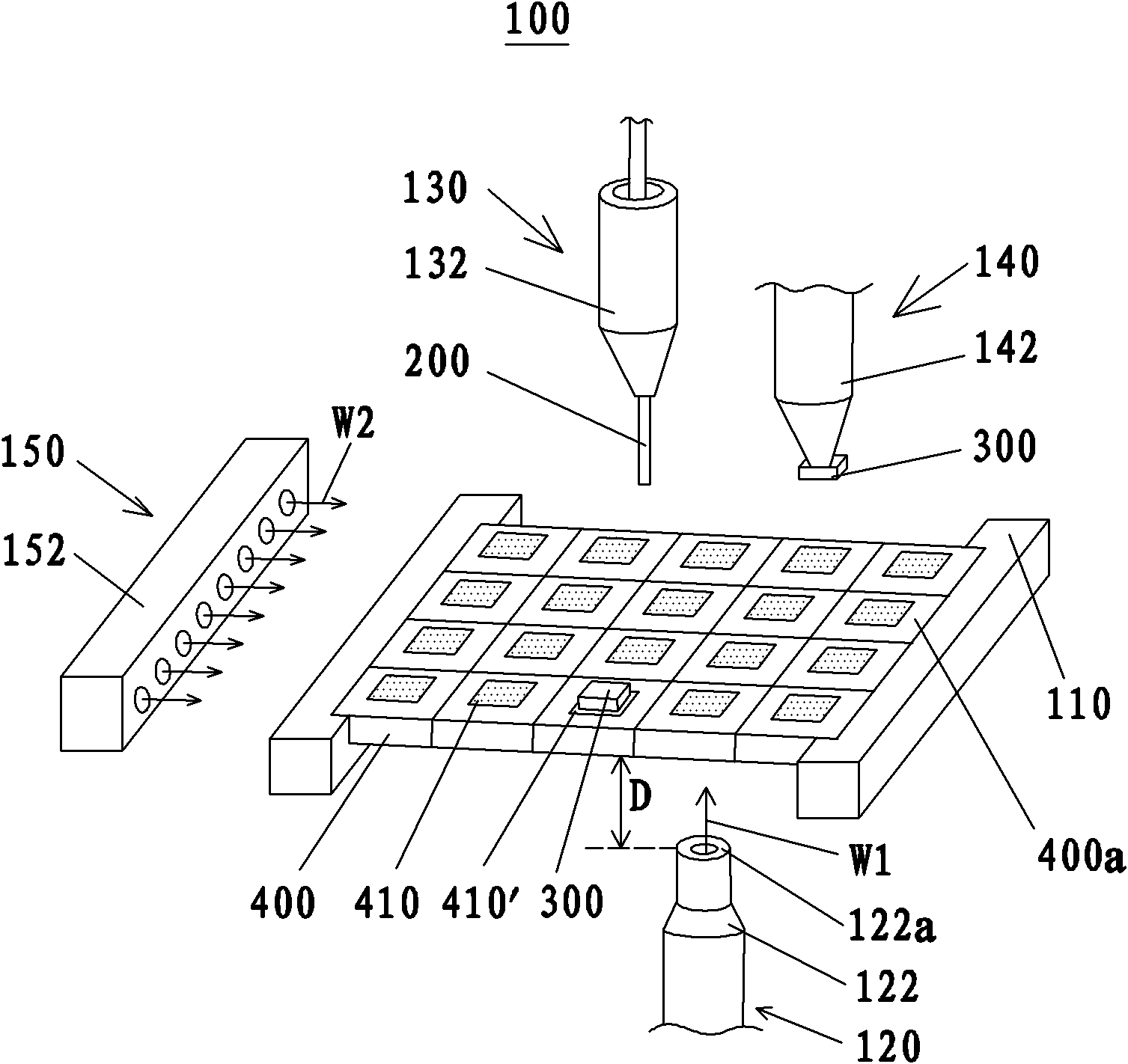
[0044] figure 1 It is a schematic diagram of a chip bonding system according to an embodiment of the present invention. Please refer to figure 1 , the chip bonding system 100 of this embodiment is suitable for fixing the plurality of chips 300 on the plurality of bonding pads 410 of the substrate 400 by using the solder 200 . The chip bonding system 100 of this embodiment includes a substrate positioning module 110 , a heating module 120 , a solder supply module 130 and a chip carrying module 140 . The substrate 400 may have a plurality of unit regions 400a, and one pad 410 is disposed on each unit region 400a. The solder 200 includes eutectic solder, and the material of the eutectic solder includes gold-tin alloy or silver-tin alloy.

[0045]The substrat...


PUM


Abstract

The invention discloses a chip bonding system, which comprises a substrate positioning module, a heating module, a welding flux supply module and a chip carrying module, wherein a substrate is positioned on the substrate positioning module and is provided with a plurality of weld pads; the heating module is arranged on a frame of the bonding system in a manner of moving relative to the substrate positioning module for heating each weld pad one by one; the welding flux supply module is provided with a welding flux and is arranged on the frame of the bonding system in a manner of moving relative to the substrate positioning module for supplying welding fluxes to the heated weld pads; and the chip carrying module is arranged on the frame of the bonding system in a manner of moving relative to the substrate positioning module for separately carrying chips one by one and making the chips contact with the welding fluxes molten on the weld pads. The invention further discloses a chip bondingmethod. By adopting the chip bonding system and method, chips can be well bonded on the substrate and the chip bonding quality is stable.

Description

technical field [0001] The invention relates to a chip bonding system and a chip bonding method, in particular to a chip bonding system and a chip bonding method that can provide high chip bonding quality and high productivity. Background technique [0002] There are two ways to fix the chip on the substrate by eutectic solder. One way is as follows: First, a layer of eutectic solder, such as gold-tin alloy or silver-tin alloy, is evaporated or sputtered on the back of the chip. Next, plate a layer of gold on the pads on the substrate; then, place the substrate on a heating plate and heat it to the melting point of the eutectic solder, press the chip onto the pads and make the gold on the pads and the eutectic solder on the chip Then, the temperature of the substrate is lowered below the melting point of the eutectic solder to solidify the eutectic solder, that is, the die bonding operation is completed. However, when the eutectic solder is plated on the back of the chip, ...

Claims


Application Information

Patent Timeline
Patent Type & Authority Applications(China)
IPC IPC(8): H01L21/60
CPCH01L24/83H01L24/743H01L2924/01322H01L24/75
Inventor 何永基吕孝文林积锁
Owner 何永基
Why Eureka
Try Eureka