Method for manufacturing selective emitter battery

A manufacturing method and emitter technology, applied in circuits, electrical components, climate sustainability, etc., can solve the problems of yield impact and equipment accuracy requirements, meet the requirements of reducing equipment accuracy, and achieve self-alignment , The effect of simplifying the process

Inactive Publication Date: 2011-09-14
JETION SOLAR HLDG
View PDF6 Cites 12 Cited by
  • Summary
  • Abstract
  • Description
  • Claims
  • Application Information

AI Technical Summary

Problems solved by technology

[0006] The above process requires an alignment operation when printing silver paste, so the accuracy of the equipment is very high, resulting in a certain impact on the yield

Method used


Image

  • Method for manufacturing selective emitter battery
  • Method for manufacturing selective emitter battery
  • Method for manufacturing selective emitter battery

Examples


Embodiment Construction

[0030] In order to make the above objects, features and advantages of the present invention more comprehensible, the embodiments of the present invention will be further described in detail below in conjunction with the accompanying drawings and specific implementation methods.

[0031] The invention provides a method for making an SE battery, such as figure 1 shown, including the following steps:

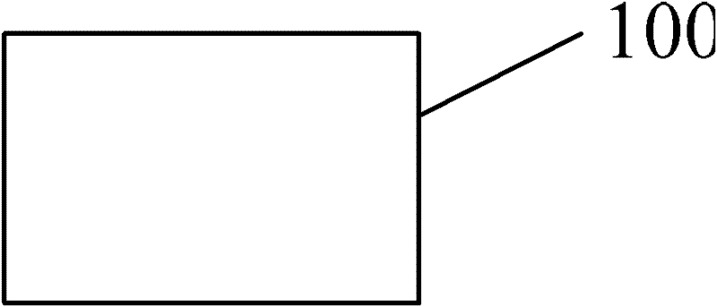
[0032] S10, providing a semiconductor substrate 100 (see figure 2 ).

[0033] The semiconductor substrate 100 is generally monocrystalline silicon or polycrystalline silicon, and may also be monocrystalline silicon germanium or polycrystalline silicon germanium, etc.; the semiconductor substrate may be a P-type substrate or an N-type substrate.

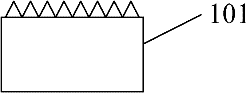
[0034] S20, making texture on the semiconductor substrate 100 (see image 3 ).

[0035] Texture can be made only on the front side of the semiconductor substrate, or can be made on both sides of the semiconductor substrate simultaneou...


PUM

PropertyMeasurementUnit
thicknessaaaaaaaaaa
thicknessaaaaaaaaaa
thicknessaaaaaaaaaa

Abstract

The invention discloses a method for manufacturing a selective emitter battery. The method comprises the following steps of: providing a semiconductor substrate; flocking on the semiconductor substrate; performing diffusion and doping on the semiconductor substrate and forming a diffusion layer on the front face of the semiconductor substrate, wherein the diffusion layer comprises a high-doping-concentration layer on a surface layer and a low-doping-concentration layer on an inner layer; trimming the diffused semiconductor substrate; forming a silver paste electrode which corresponds to a grid line on the surface of the diffusion layer and forming a back electrode and a back electric field at the bottom of the semiconductor substrate; plating a conductive metal on the surface of the silver paste electrode; etching and removing the high-doping-concentration layer exposed on the front face of the semiconductor substrate by taking the conductive metal as a mask; depositing an anti-reflective film on the front face of the semiconductor substrate; and removing the anti-reflective film on the top surface of a part to be subjected to electrode welding of the conductive metal. In the method, the conductive metal is plated on the silver paste electrode and is taken as the mask for removing the high-doping-concentration layer, so that the requirement for the equipment accuracy is lowered and the production yield of an SE (Spray Etching) battery is increased.

Description

technical field [0001] The invention relates to the field of photovoltaic technology, in particular to a method for manufacturing a selective emitter battery. Background technique [0002] At present, the development of high-efficiency cell technology is the key to improving the efficiency of solar cells. The relatively mature high-efficiency battery technology is dominated by selective emitter (SE) batteries. [0003] The structure of the SE cell has two characteristics: 1) a highly doped deep diffusion region is formed in the gate line contact area (below the gate line and its vicinity, and the emitter region is subsequently formed); 2) a low doped shallow diffusion region is formed in other areas. By selectively doping the emitter region, the effects of different diffusion square resistances are realized in the gate line contact region and other regions, and the series resistance is reduced. [0004] An existing method for making an SE battery is as follows (taking a P-...

Claims


Application Information

Patent Timeline
Patent Type & Authority Applications(China)
IPC IPC(8): H01L31/18
CPCY02P70/50
Inventor 张忠钱明星
Owner JETION SOLAR HLDG
Why Eureka
Try Eureka