Coating and developing apparatus and developing method
A technology of a developing device and a developing method, which is applied in the field of coating-developing device and developing, can solve the problems of increased processing cost and large amount of developer evaporation, and achieve the effect of suppressing the reduction of productivity
- Summary
- Abstract
- Description
- Claims
- Application Information
AI Technical Summary
Problems solved by technology
Method used
Image
Examples
no. 1 Embodiment approach
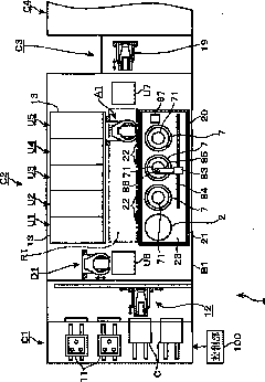
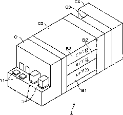
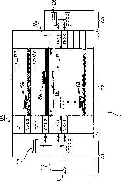
[0053] First, a coating-developing apparatus 1 to which the developing system of the present invention is applied will be described. figure 1 A plan view showing a resist pattern forming system in which an exposure device C4 is connected to a coating-developing device 1, figure 2 is a perspective view of the system. also, image 3 is a longitudinal sectional view of the system. In this coating-developing apparatus 1, a transfer area C1 is provided, and a transfer arm 12 takes out a wafer W from a closed carrier C placed on a stage 11 and transfers it to a processing area C2, and the transfer arm 12 transfers the wafer W from the processing area C2 to the processing area C2. The zone C2 receives the processed wafer W and returns it to the carrier C.
[0054] Such as figure 2 As shown, in the above-mentioned processing area C2, in this example, the first area (DEV layer) B1 for performing the development process, the first area (DEV layer) B1 for performing the forming pro...
no. 2 Embodiment approach
[0087] then, Figure 12 Another configuration example of the first area (DEV layer) B1 is shown. In this example, the components of the shelf unit U1 are constituted as a developing unit 101 . In addition, a unit corresponding to the first developing unit 20 is configured as a cleaning processing unit 2A. The cleaning processing unit 2A has the same configuration as the developing unit 20 except that four sets of cleaning units 7 are arranged in the horizontal direction and no developing unit 2 is provided.
[0088] Respectively refer to as longitudinal section side view, transverse section top view Figure 13 , Figure 14 , to describe the differences between the developing unit 101 and the developing unit 2. In the developing unit 101 , the interior of the frame 102 is partitioned up and down by a partition plate 103 , and a cooling plate 105 is provided on the upper side of the partition plate 103 . The cooling plate 105 is formed in a substantially circular shape and ...
no. 3 Embodiment approach
[0092] Next, about Figure 15 Still another example of the configuration of the first block B1 shown will be described focusing on differences from the first embodiment. exist Figure 15 In the first block B1 of , a developing unit 20A is provided instead of the developing unit 20 , and a transport member 111 for transporting the wafer W from the developing unit 2 to the cleaning unit 7 is provided on the developing unit 20A. Figure 16 A perspective view showing the inside of the housing 21 of the developing unit 20A. A guide 112 extending along the arrangement direction of the cleaning assembly 7 and the developing assembly is formed on the base 23 . The horizontal movement part 113 constituting the transport member 111 moves horizontally along the extending direction of the guide 112 . A lift unit 114 configured to be able to move up and down is connected to the horizontal movement unit 113 , and a transport arm 115 is provided on the lift unit 114 . The transport arm 1...
PUM
| Property | Measurement | Unit |
|---|---|---|
| coating thickness | aaaaa | aaaaa |
| diameter | aaaaa | aaaaa |
Abstract
Description
Claims
Application Information
 - R&D
- Intellectual Property
- Life Sciences
- Materials
- Tech Scout
- Unparalleled Data Quality
- Higher Quality Content
- 60% Fewer Hallucinations
Browse by: Latest US Patents, China's latest patents, Technical Efficacy Thesaurus, Application Domain, Technology Topic, Popular Technical Reports.
© 2025 PatSnap. All rights reserved.Legal|Privacy policy|Modern Slavery Act Transparency Statement|Sitemap|About US| Contact US: help@patsnap.com


