Manufacturing method of electronic device package, electronic device package, and oscillator

A technology of electronic devices and manufacturing methods, applied in semiconductor/solid-state device manufacturing, electrical solid-state devices, manufacturing microstructure devices, etc., capable of solving alignment restrictions between the base substrate 41 and the cover substrate 42, the impact of product production quantity, and wafer surface bonding Solve problems such as strength deviation, achieve the effect of firm joint strength, suppress warpage, and increase charge amount

Inactive Publication Date: 2011-09-21
SEIKO INSTR INC
View PDF11 Cites 10 Cited by
  • Summary
  • Abstract
  • Description
  • Claims
  • Application Information

AI Technical Summary

Problems solved by technology

First of all, there is a problem that when performing anodic bonding, although the positive electrode probe 52 is brought into contact with a part of the metal film 49 as the bonding film, when the sheet resistance of the metal film 49 is high, it is difficult to attach the lid as the wafer. The entire surface of the substrate 42 is kept at the same potential, resulting in variations in bonding strength within the wafer plane
Therefore, there is a problem that there is a great restriction on the alignment between the base substrate 41 and the cover substrate 42.
Especially for a package with a pattern formed on the lid substrate 42 side, there is a problem that the limitation of alignment has a great influence on the production quantity of products on a wafer.

Method used


Image

  • Manufacturing method of electronic device package, electronic device package, and oscillator
  • Manufacturing method of electronic device package, electronic device package, and oscillator
  • Manufacturing method of electronic device package, electronic device package, and oscillator

Examples


Embodiment Construction

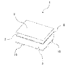
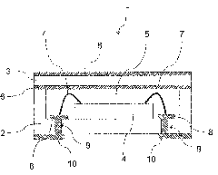
[0031] Below, refer to Figure 1 to Figure 5 Embodiments of the present invention will be described. Such as figure 1 and figure 2 As shown, the electronic device package 1 of the present embodiment is formed in a box shape in which two layers of a base substrate 2 and a lid substrate 3 are laminated, and is a surface mount type package in which an electronic device 4 is accommodated in an internal cavity 5 . The electronic device 4 is LSI, MEMS, a sensor, a piezoelectric vibrator, or a composite of these.

[0032] Both the base substrate 2 and the lid substrate 3 are insulating substrates made of an insulating material containing movable ions, such as soda lime glass. exist figure 1 and figure 2 In the illustrated example, a rectangular recess (cavity) 5 for accommodating an electronic device 4 is formed on the base substrate 2, and the lid substrate 3 is formed in a flat plate shape. The concave portion 5 is a concave portion that becomes a cavity 5 for housing the...


PUM


Abstract

The invention provides a manufacturing method of an electronic device package, an electronic device package and an oscillator, capable of bonding an insulator base substrate and an insulator cover substrate together via a metal film by anodic bonding in a stable manner. The electronic device package manufacturing method includes: forming a metal film on both surfaces of the cover substrate so that the metal film on one surface and the metal surface on the other surface conduct with each other; aligning and superimposing the cover substrate and the base substrate; and bonding the base substrate and the cover substrate together via the metal film by anodic bonding by bringing a negative electrode plate into contact with the base substrate on an entire surface opposite to a surface bonded to the cover substrate, bringing a positive electrode plate into contact with the cover substrate on an entire surface opposite to a surface bonded to the base substrate, and applying a voltage between the positive and negative electrode plates. The base substrate and the cover substrates can be thus bonded together via the metal film by anodic bonding in a stable manner.

Description

technical field [0001] The present invention relates to a surface mount type (SMD) package that seals an electronic device in a cavity formed between two substrates that are bonded. A configuration for anodic bonding of two substrates is proposed in particular. Background technique [0002] In recent years, in mobile phones and portable information terminal devices, electronic devices in small, surface-mounted packages have been widely used. Among them, there are also many packaged components that require a hollow cavity structure, such as vibrators, MEMS, gyro sensors, acceleration sensors, and the like. In a package with a hollow cavity structure, a structure in which a base substrate of an insulator and a lid substrate of an insulator are bonded via a metal film is known. Furthermore, eutectic bonding, seam bonding, and anodic bonding are also known as bonding methods (see Patent Document 1). [0003] Here, a conventional method for manufacturing a package in which a b...

Claims


Application Information

Patent Timeline
Patent Type & Authority Applications(China)
IPC IPC(8): H01L21/52H01L21/60H01L23/043H01L23/10H03H3/02
CPCH01L24/97B81C2203/0118H01L2224/48091B81C1/00269B81C2203/031H01L2224/48227H01L2924/01322H01L2924/14H01L2924/1461H01L2924/15787H01L2924/00014H01L2924/00H01L23/043
Inventor 吉田宜史
Owner SEIKO INSTR INC
Why Eureka
Try Eureka