Semiconductor memory device

A memory and semiconductor technology, applied in static memory, read-only memory, information storage, etc., to achieve the effect of improving the correction ability

Active Publication Date: 2014-04-23
KIOXIA CORP
View PDF5 Cites 0 Cited by
  • Summary
  • Abstract
  • Description
  • Claims
  • Application Information

AI Technical Summary

Problems solved by technology

Therefore, the probability of existence of the above-mentioned faults in the memory device increases dramatically

Method used


Image

  • Semiconductor memory device
  • Semiconductor memory device
  • Semiconductor memory device

Examples


Embodiment Construction

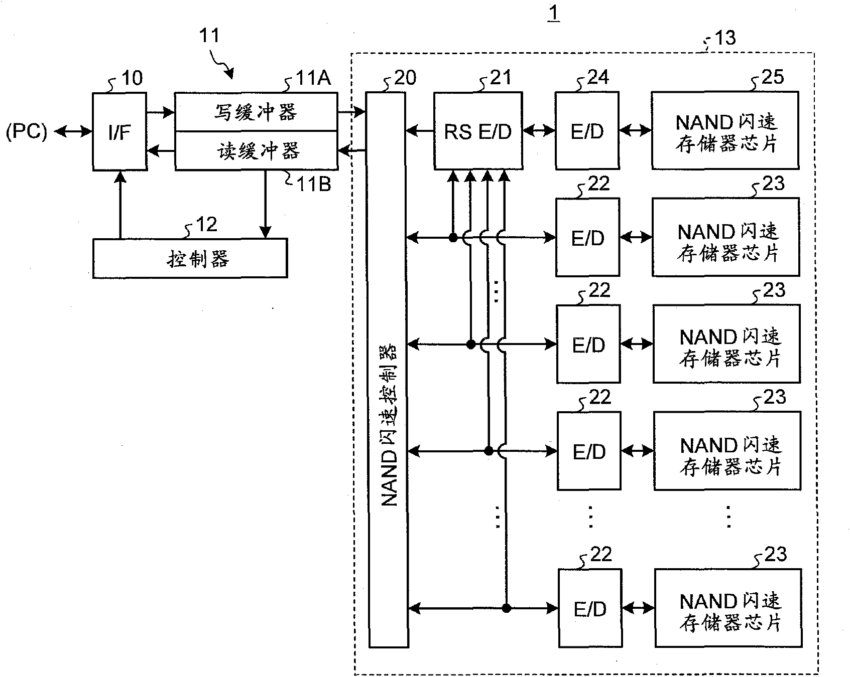
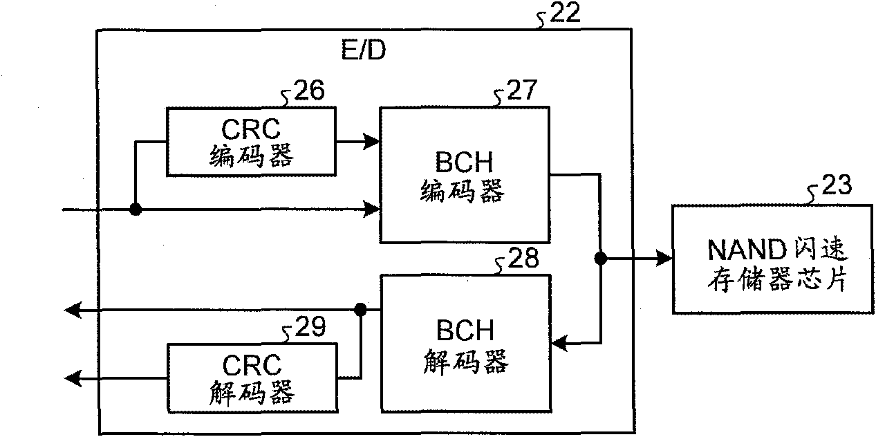
[0031] Exemplary embodiments of semiconductor memory devices will be described in detail with reference to the accompanying drawings. In this embodiment, a memory chip storing an error correction code to recover damage of a large data block is provided in a semiconductor memory device in which a plurality of memory chips are mounted. When data is corrupted in a large data block, the data is recovered by using the error correction code. The error correction code for recovering damage of a large data block is also used as an error correction code for correcting an error in a small data block, and error correction between memory chips and error correction in a page are performed arbitrarily and repeatedly, so Improved error correction capability.

[0032] figure 1 is a block diagram showing the configuration of the semiconductor memory device 1 applicable to the embodiment. exist figure 1 In an example, a semiconductor memory device 1 includes an interface (I / F) 10 , a buffer...


PUM


Abstract

A CRC code is generated from an original data, a BCH code is generated with respect to the original data and the CRC code, and the original data, the CRC code, and the BCH code are recorded in pages selected from different planes of a plurality of memory chips. An RS code is generated from the original data across pages, a CRC code is generated with respect to the RS code, a BCH code is generated with respect to the RS code and the CRC code, and the RS code, the CRC code, the BCH code are recorded in a memory chip different from a memory chip including the original data. When reading data, error correction is performed on the original data by using the BCH code, and then CRC is calculated. If the number of errors is the number of errors that is correctable by erasure correction using the RS code, the original data is corrected by the erasure correction. If the number of errors exceeds an erasure correction capability of the RS code, normal error correction using the RS code is performed, and further error correction using the BCH code is performed.

Description

[0001] Cross References to Related Applications [0002] This application is based on and claims priority from Japanese Patent Application No. 2010-069012 filed March 24, 2010; the entire contents of which are hereby incorporated by reference. technical field [0003] Embodiments described herein relate generally to semiconductor memory devices. Background technique [0004] The NAND flash memory chip includes a large number of memory cells in its chip, converts data into charges and records the data in the memory cells. The interior of the chip is divided into multiple memory blocks. In the memory block, there is a unit called a block as a unit of deleting data, and there is also a unit called a page which is formed by further dividing a block and is a unit of reading / writing data. [0005] NAND flash memory records data according to its charge amount. Therefore, as time elapses, the charges are discharged, whereby errors occur in recorded data. In order to correct data...

Claims


Application Information

Patent Timeline
Patent Type & Authority Patents(China)
IPC IPC(8): G11C29/44
CPCH03M13/2906G06F11/1068G11C16/10G06F11/1072G11C2029/0411H03M13/29G06F11/1076G06F11/1012G11C29/42G11C16/06G06F11/10G06F12/16G11C29/52H03M13/1515
Inventor 菅野伸一
Owner KIOXIA CORP
Why Eureka
Try Eureka