Drive device, display panel module, display device and method for manufacturing drive device

A driving device and display device technology, applied in the direction of static indicators, optics, instruments, etc., can solve the problems of excessive wiring, increase the use of carrier tape, and can not achieve cost reduction, etc., to achieve the effect of low heat generation

Inactive Publication Date: 2011-09-28
PANASONIC CORP
View PDF8 Cites 6 Cited by
  • Summary
  • Abstract
  • Description
  • Claims
  • Application Information

AI Technical Summary

Problems solved by technology

[0026] In other words, for a small display, cost reduction can be achieved, but for a large or high-resolution display, since the wiring of the control signal from the semiconductor element for driving the display increases, it is necessary to increase the carrier tape. As a result, the cost increases and the effect of cost reduction cannot be obtained

Method used


Image

  • Drive device, display panel module, display device and method for manufacturing drive device
  • Drive device, display panel module, display device and method for manufacturing drive device
  • Drive device, display panel module, display device and method for manufacturing drive device

Examples


Embodiment 1

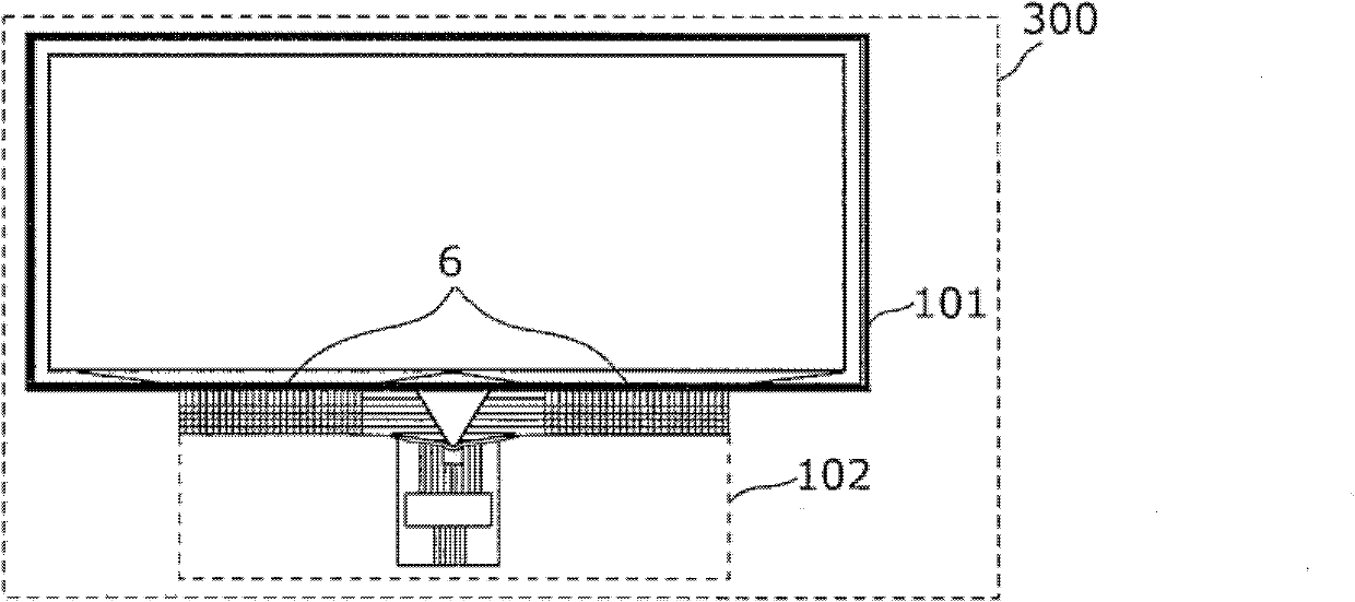
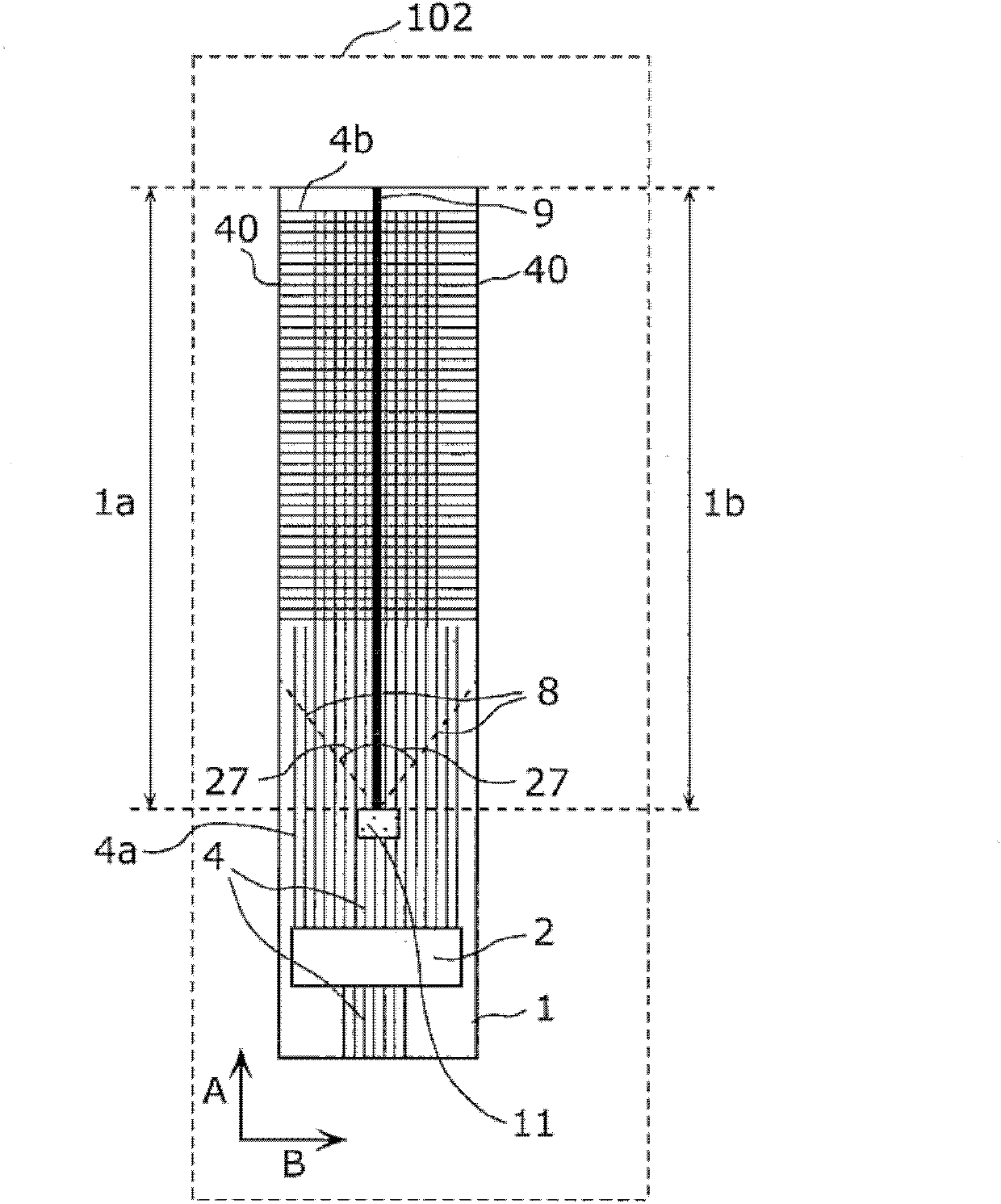
[0115] Figure 1A is a plan view showing the configuration of the display screen module 300 in this embodiment. Figure 1B It is a plan view showing the shape of the driving device 102 in this embodiment before being attached to the liquid crystal panel 101 . exist Figure 1A Among them, the display module 300 is composed of a liquid crystal screen 101 and a driving device 102 , the driving device 102 is connected to the wiring 6 on the substrate included in the liquid crystal screen 101 and drives the liquid crystal screen 101 . The driving device 102 is mounted on the outer edge of the liquid crystal panel 101, and includes the film 1 on which the wiring 4 and the circuit element 2 are mounted.

[0116] In addition, although the display panel is described as a liquid crystal panel here, the same effect can be obtained also in a thin display such as an organic electroluminescent panel or a plasma display.

[0117] Such as Figure 1B It is shown that the driving device 102...

Deformed example 1

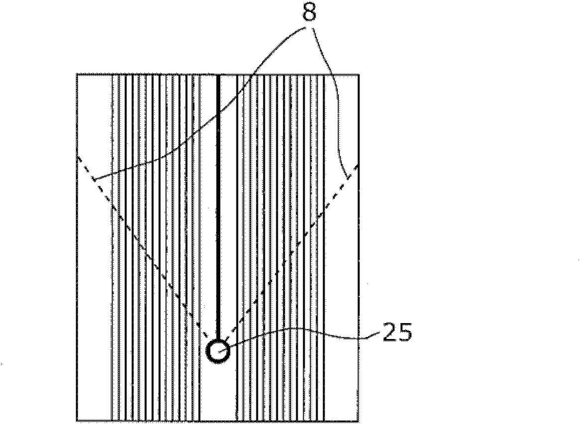
[0137] use Figure 5A to Figure 6C Modifications related to measures against disconnection of the wiring 4 on the thin film 1 in the driving device 102 of the present embodiment will be described.

[0138] Figure 5A is a plan view showing the shape of the driving device 102 before being mounted on the liquid crystal panel 101, Figure 5B The diagram around the bending position 8 of the driving device 102 is shown enlarged.

[0139] Such as Figure 5B As mentioned above, by setting the wiring strengthening part 20 that changes the width of the wiring 4 at the intersection of the wiring 4 and the bending position 8 on the film 1, specifically, by making the line width of the wiring 4 at the bending position 8 of the film 1 By widening, the effect of reducing the disconnection failure rate of the wiring 4 in the drive device 102 can be obtained.

[0140] Figure 6A is a plan view showing the shape of the driving device 102 before being mounted on the liquid crystal panel 10...

Embodiment 2

[0145] Figure 7A is a plan view showing the configuration of the display screen module 301 in this embodiment. Figure 7B It is a plan view showing the shape of the driving device 103 in this embodiment before being attached to the liquid crystal panel 101 .

[0146] exist Figure 7A Among them, the display module 301 is composed of a liquid crystal screen 101 and a driving device 103 . The driving device 103 is connected to the wiring 6 on the substrate included in the liquid crystal screen 101 and drives the liquid crystal screen 101 . The driving device 103 is mounted on the outer edge of the liquid crystal panel 101, and includes the film 1 on which the wiring 4 and the circuit element 2 are mounted. Moreover, the display screen module 301 of this embodiment also constitutes as Figure 4A to Figure 4C display device.

[0147] Such as Figure 7B It is shown that the driving device 103 utilizes the film 1 as a base material, mounts the circuit element 2 on the film 1 ,...


PUM


Abstract

Provided is a drive device, display panel module, display device and method for manufacturing a drive device, which make it possible to reduce the number of drive circuit elements without reducing the number of display panels to be taken out, and without increasing interconnection regions on a film. Specifically, provided is a drive device which is provided with a film (1), on which interconnections (4) and a circuit element (2) are mounted, and drives a display panel. The drive device is provided with a first film portion (1a) and second film portion (1b) in the film (1) which are separated from each other by an incision (9) made therein, and each of the first and second film portions (1a and 1b) is connected to the display panel while having been folded at least once.

Description

technical field [0001] The present invention relates to a driving device (display driving device) mounted on a display screen such as a liquid crystal panel or an organic electroluminescent screen, a display module using the driving device, a display device, and a method for manufacturing the driving device. Background technique [0002] In recent years, display devices mounted on display devices have gradually shifted from devices using cathode ray tubes to devices using liquid crystal panels (display screens), which have low power consumption. And save space and other advantages. [0003] However, at present, the price of an LCD screen is about several times that of a cathode ray tube. In order to further expand the market for LCD screens, it is essential to reduce the cost of LCD screens and peripheral equipment. [0004] As the size of the display screen progresses, the Figure 15A In the shown display device, the number of semiconductor devices 54 used increases, and a...

Claims


Application Information

Patent Timeline
Patent Type & Authority Applications(China)
IPC IPC(8): G09G3/20G09G3/36G02F1/1345H01L23/538
CPCG02F2001/13456G02F1/13452G02F1/1345G02F1/13456Y10T29/4913
Inventor 小川宗彦北山裕己石川智也小岛宽西和义须山透
Owner PANASONIC CORP
Why Eureka
Try Eureka