High-efficient full-spectrum silicon-based double-knot photovoltaic cell

A photovoltaic cell, full-spectrum technology, applied in the field of solar energy applications, can solve the problems of large investment, long processing time, unfavorable production efficiency, etc., and achieve the effects of high production efficiency, low production cost, and overcoming the discontinuity of the interface electric field.

Inactive Publication Date: 2013-07-31
XI AN JIAOTONG UNIV
View PDF4 Cites 0 Cited by
  • Summary
  • Abstract
  • Description
  • Claims
  • Application Information

AI Technical Summary

Problems solved by technology

However, the bottom cell of the battery adopts a long-term high-temperature diffusion process, and the processing time is long, which is not conducive to improving production efficiency, reducing production costs and silicon wafer thickness, and theoretical calculations show that: a double-junction battery composed of two units can basically Using the entire solar spectrum can greatly improve the photoelectric conversion efficiency of the battery. When a triple-junction photovoltaic battery is composed of three units, if the increased efficiency of the battery is compared with the increased workload, from a technical and economic point of view, the investment is greater than output

Method used


Image

  • High-efficient full-spectrum silicon-based double-knot photovoltaic cell

Examples


Embodiment Construction

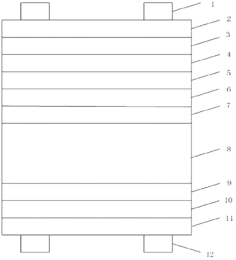
[0016] refer to figure 1 Shown: 1. front silver electrode, 2. front TCO conductive film, 3. front p-type nano-silicon layer, 4. i-type nano-silicon layer, 5. front n-type nano-silicon layer, 6. p-type nano-silicon layer, 7. Front nano-silicon buffer layer, 8. n-type single crystal silicon, 9. Back nano-silicon buffer layer, 10. Back n-type nano-silicon layer, 11. Back TCO conductive film, 12. Back silver electrode.

[0017] by figure 1 The sequence shown is an example, and the preparation process includes the following steps:

[0018] (1) Select an n-type single crystal silicon wafer, the resistivity of the silicon wafer is 1-3 Ω·cm, the thickness of the silicon wafer is about 200 μm, and the silicon wafer is polished with a concentration of 20% sodium hydroxide solution, and the silicon wafer after cleaning The sheet is a polished sheet, which requires a bright surface without spots, scratches, or water marks.

[0019] (2) Deposit a nano-buffer layer and an n-type nano-sil...


PUM

PropertyMeasurementUnit
optical band gapaaaaaaaaaa
thicknessaaaaaaaaaa

Abstract

The invention discloses a high-efficient full-spectrum silicon-based double-knot photovoltaic cell; the cell is sequentially composed of the following components from top to bottom: a positive silver electrode, a positive TCO (transparent conducting film) conducting film, a positive p-type nano silicon layer, an i-type nano silicon layer, a positive n-type nano silicon layer, a p-type nano silicon layer, a positive nano silicon buffer layer, a n-type monocrystalline silicon, a back nano silicon buffer layer, a back n-type nano silicon layer, a back TCO conducting film and a back silver electrode. A bottom cell in a cell with the structure has partial advantages of an HIT (heterojunction with intrinsic thinlayer) photovoltaic cell, and a top battery in the cell has the characteristics of anano silicon film photovoltaic cell. The photovoltaic cell in the structure is good in junction property and high in open-circuit voltage; and meanwhile, a reflected light from the ground can be usedby a symmetrical cell structure to obtain high photoelectric conversion efficiency.

Description

technical field [0001] The invention relates to a new structure of a photovoltaic cell, which belongs to the field of solar energy applications. Background technique [0002] As a photoelectric conversion device that directly utilizes solar energy, photovoltaic cells have been developing in two directions. One is to reduce the production cost of photovoltaic cells, and the other is to improve the photoelectric conversion efficiency of photovoltaic cells. At the same time, the stability of photovoltaic cells is also a concern. [0003] Crystalline silicon photovoltaic cells have the advantages of high efficiency and stable performance, and have always been the main force of photovoltaic power generation. However, high temperature diffusion is required in the manufacturing process of crystalline silicon photovoltaic cells, which increases the stress of the battery, which is not conducive to the thinning of the battery sheet thickness, resulting in The cost of generating elect...

Claims


Application Information

Patent Timeline
Patent Type & Authority Patents(China)
IPC IPC(8): H01L31/078H01L31/0352
CPCY02E10/50
Inventor 王鹤杨宏帅争峰
Owner XI AN JIAOTONG UNIV
Why Eureka
Try Eureka