Light emitting diode (LED) pixel unit device structure and preparation method thereof

A device structure and pixel unit technology, which is applied in the direction of electrical components, electric solid devices, semiconductor devices, etc., can solve the problems of large distance between LED chip units, different LED tube attenuation curves, poor color consistency of the display screen, etc., to reduce the size of the device Package area, solve the light blocking problem of pads and leads, and improve the effect of color consistency

Inactive Publication Date: 2011-10-12
ENRAYTEK OPTOELECTRONICS
View PDF2 Cites 39 Cited by
  • Summary
  • Abstract
  • Description
  • Claims
  • Application Information

AI Technical Summary

Problems solved by technology

However, since the light source of LEDs is composed of different colors, slight changes in the arrangement of LEDs may change the color of the screen or reduce the brightness.
[0007] Moreover, because in the prior art, red (R), green (G), and blue (B) LEDs are generally packaged separately and then arranged together, the package structure is not compact, and the distance between the LED chip units is relatively large.
[0008] Bare chip technology (mainly chip-on-board packaging technology and flip-chip technology) can package RGB three-color LEDs together and improve the resoluti

Method used


Image

  • Light emitting diode (LED) pixel unit device structure and preparation method thereof
  • Light emitting diode (LED) pixel unit device structure and preparation method thereof
  • Light emitting diode (LED) pixel unit device structure and preparation method thereof

Examples


Embodiment Construction

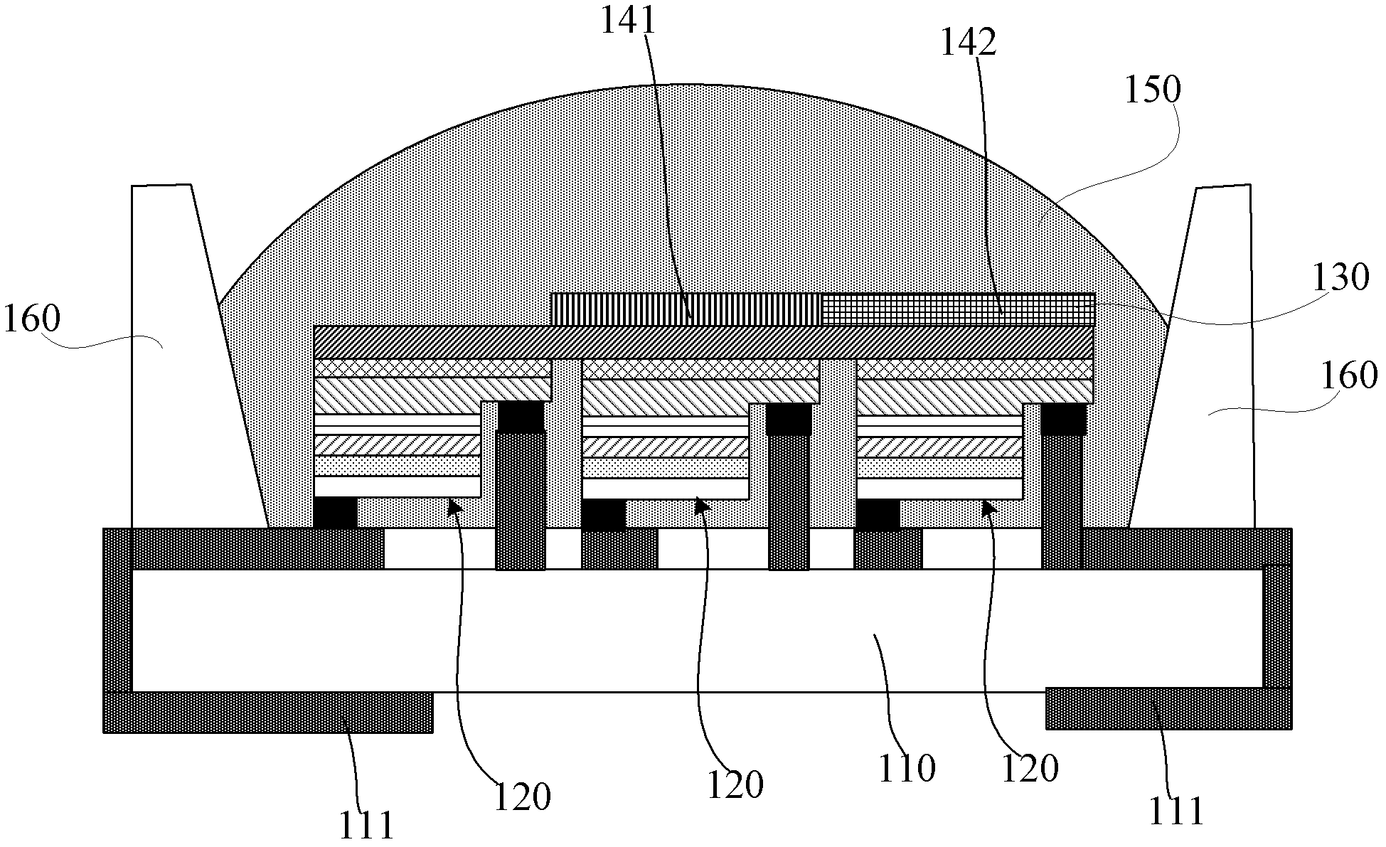
[0044] The structure of the LED pixel unit device proposed by the present invention and its preparation method will be further described in detail below in conjunction with the accompanying drawings and specific embodiments. Advantages and features of the present invention will be apparent from the following description and claims. It should be noted that all the drawings are in very simplified form and use imprecise ratios, which are only used for the purpose of conveniently and clearly assisting in describing the embodiments of the present invention.
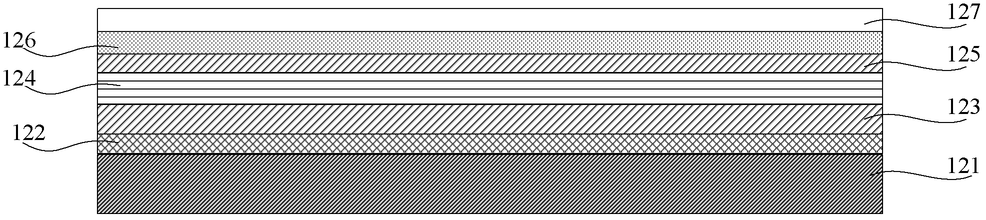
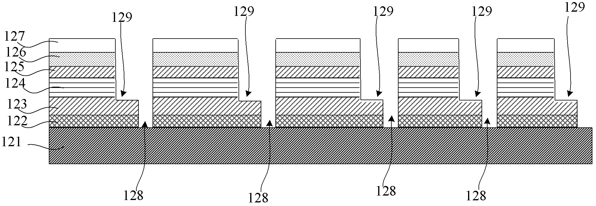
[0045]The core idea of ​​the present invention is to provide a LED pixel unit device structure, and package three LED chip units that are connected by the same substrate but completely isolated electrically in a flip-chip structure, thereby reducing the device packaging area and improving The resolution of the LED display screen is improved; and the structures of the three LED chip units are exactly the same. By coating the bl...


PUM


Abstract

The invention discloses a light emitting diode (LED) pixel unit device structure. Three blue LED chip units which are connected with one another through the same substrate and electrically isolated from one another are inversely assembled with one another, so a package area is reduced and the resolution of an LED display screen is improved; the structures of the LED chip units are the same; greenfluorescent powder and red fluorescent powder are coated on two of the LED chip units respectively, so the two LED chip units can emit green light and red light respectively; therefore, during use, the attenuation of the LED chip units are consistent, and the color consistency of the display screen is enhanced. The invention also discloses a preparation method of the structure. An LED module is inversely arranged on a heat conducting substrate, so steps of chip bonding and gold line bonding are omitted, the cost is reduced, manufacturing efficiency is improved, the problem that a welding diskand a lead wire in an LED package block light is solved, the light emergent efficiency of an LED is improved greatly, package space is saved, and the LED package can be further miniaturized and integrated.

Description

technical field [0001] The invention relates to the technical field of LED preparation, in particular to an LED pixel unit device structure and a preparation method thereof. Background technique [0002] A light-emitting diode (LED, Light Emitting Diode) is a semiconductor solid-state light-emitting device, which uses a semiconductor PN junction as a light-emitting material, and can directly convert electricity into light. When a forward voltage is applied to both ends of the semiconductor PN junction, the minority carriers injected into the PN junction recombine with the majority carriers, and excess energy is released to cause photon emission, which directly emits red (R) and orange colors. , yellow, green (G), cyan, blue (B), purple light. [0003] With the gradual maturity of ultra-high brightness LED technology, the price continues to drop, and because of its use of three primary colors, good color reproduction, low power consumption, and long life, short and thin, and...

Claims


Application Information

Patent Timeline
IPC IPC(8): H01L25/075H01L33/48H01L33/62H01L33/50H01L33/00
CPCH01L2224/14
Inventor 肖德元程蒙召张汝京
Owner ENRAYTEK OPTOELECTRONICS
Why Eureka
Try Eureka