Aqueous dispersion system and method for etching polysilicon wafer

A technology for water-based dispersion and polycrystalline silicon wafers, which is applied to the etching field of water-based dispersion systems and polycrystalline silicon wafers, and can solve problems such as increased cost and production environment hazards.

Inactive Publication Date: 2011-11-16
EI DU PONT DE NEMOURS & CO
View PDF5 Cites 5 Cited by
  • Summary
  • Abstract
  • Description
  • Claims
  • Application Information

AI Technical Summary

Problems solved by technology

Although the above method avoids the use of hydrofluoric acid, the high concentration of alkali in the solution will not only bring harm to the production environment, but also increase the cost of waste disposal for enterprises
[0008] In addition, there is still room for improvement in the light reflectance of the polysilicon wafers made by the existing polysilicon wafer etching method

Method used


Image

  • Aqueous dispersion system and method for etching polysilicon wafer
  • Aqueous dispersion system and method for etching polysilicon wafer
  • Aqueous dispersion system and method for etching polysilicon wafer

Examples


Embodiment

[0085] Below in conjunction with embodiment further illustrate this patent application. Those skilled in the art can understand that the scope of this patent application is not limited thereto.

[0086] The polycrystalline silicon wafers used in the following comparative examples and examples were all purchased from Konca Solar Cell Co., Ltd.

Embodiment 1

[0092] Weigh 25 mg of analytically pure bismuth hydroxide powder and put it into a beaker filled with 50 ml of deionized water. Ultrasonic breaker (SONICS, Vibro-cell TM VCX 130) dispersed for 30min, then added 0.5mg of C 18 h 29 SO 3 Na surfactant and 1 mg of C 16 f 33 C 2 h 4 (C 2 h 4 O) 8 Surfactant H, continue to sonicate for 2 hours to obtain an aqueous dispersion.

[0093] The same polycrystalline silicon wafer as in Comparative Example 1 was etched using the etching method described in Comparative Example 1 but using the aqueous dispersion system obtained in this example.

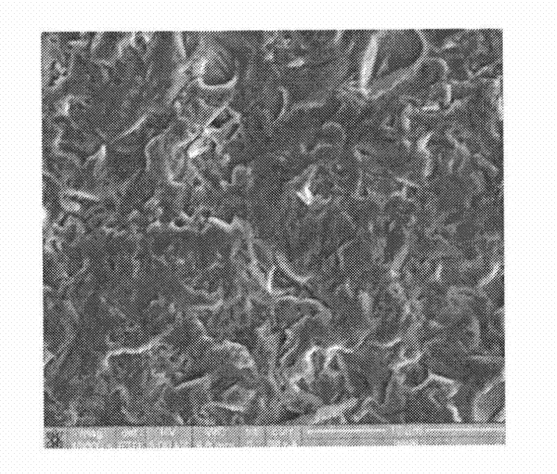
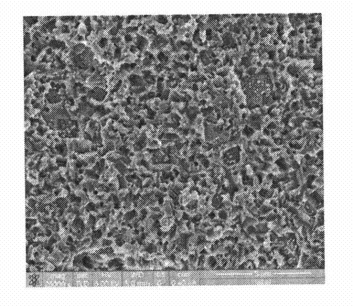
[0094] Using FEI NOVA200NanoLab SEM FIB scanning electron microscope (magnification 25000x) to observe the surface morphology of the polycrystalline silicon wafer before and after etching, the results are as follows figure 2 shown. It can be seen from the figure that the surface of the polycrystalline silicon wafer has a uniform and fine textured structure. The average reflectance (mea...

Embodiment 2

[0096] Using the dispersion method described in Example 1, 25 mg of analytically pure bismuth hydroxide powder, 0.5 mg of CH 3 (CH 2 ) 10 CH 2 SO 3 Na surfactant and 1 mg of C 16 f 33 C 2 h 4 (C 2 h 4 O) 8 The H surfactant was dispersed in 50 ml of deionized water to obtain an aqueous dispersion system.

[0097] The same polycrystalline silicon wafer as in Comparative Example 1 was etched using the etching method described in Comparative Example 1 but using the aqueous dispersion system obtained in this example.

[0098] A UV-Vis spectrophotometer (Perkin Elmer Lamda 950) was used to measure the change in reflectance before and after etching, as shown in image 3 As shown, the reflectance of the etched polysilicon wafer has a significant decrease.


PUM

PropertyMeasurementUnit
thicknessaaaaaaaaaa
electrical resistanceaaaaaaaaaa

Abstract

The invention discloses an aqueous dispersion system used for etching a polysilicon wafer. The aqueous dispersion system comprises the following components based on the total weight of the aqueous dispersion system: an aqueous medium as well as 0.0001-0.5 mol/L bismuth hydroxide and 1-5000 ppm at least one anionic or nonionic surfactant which are dispersed in the aqueous medium. The invention also discloses a method for etching the polysilicon wafer by utilizing the aqueous dispersion system and a solar polysilicon wafer cell obtained by using the method.

Description

technical field [0001] The invention relates to an aqueous dispersion system free of strong acid and strong alkaline substances for etching polycrystalline silicon wafers, a method for etching polycrystalline silicon wafers using the aqueous dispersion system and polycrystalline silicon wafers prepared by the etching method. Background technique [0002] In the solar cell industry, there are two main ways to improve the conversion rate of solar cells, one is to improve the intrinsic characteristics of solar cells, and the other is to improve the light absorption of solar cells. Anti-reflection film and suede are the main means to improve the light absorption of solar cells. The so-called suede refers to a series of regular or irregular surface shapes with different heights and sizes that exist on the surface of objects. Due to the presence of suede, the reflectivity of the surface of the object will be greatly reduced, thereby increasing its light absorption. [0003] Exis...

Claims


Application Information

Patent Timeline
Patent Type & Authority Applications(China)
IPC IPC(8): C23F1/40
Inventor 刘付胜聪周作成
Owner EI DU PONT DE NEMOURS & CO
Why Eureka
Try Eureka