Method for preparing solar cell electrodes, solar cell substrates prepared thereby, and solar cells

A solar cell and manufacturing method technology, applied in the direction of final product manufacturing, sustainable manufacturing/processing, circuits, etc., can solve the problem of weak adhesion of semiconductor wafers, reduce the number of superimposed printing, realize single printing, improve efficiency effect

Inactive Publication Date: 2011-11-16
SSCP CO LTD
View PDF5 Cites 11 Cited by
  • Summary
  • Abstract
  • Description
  • Claims
  • Application Information

AI Technical Summary

Problems solved by technology

However, in the method using photoresist, after the deposition process is completed, the metal deposition layer formed other than the portion to be the electrode needs to be removed, and the photoresist layer also needs to be removed. In addition, since the metal electrode layer is formed by deposition Formed in a manner, therefore, the adhesion to the semiconductor wafer is weak

Method used


Image

  • Method for preparing solar cell electrodes, solar cell substrates prepared thereby, and solar cells
  • Method for preparing solar cell electrodes, solar cell substrates prepared thereby, and solar cells
  • Method for preparing solar cell electrodes, solar cell substrates prepared thereby, and solar cells

Examples


Embodiment 1

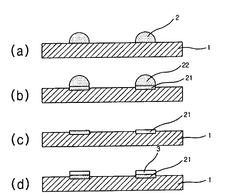
[0059] First, offset printing (gravure offset printing) was performed using a mixture for offset printing (our company's paste name SSCP1672, silver powder 68%, glass frit 17%, adhesive 10%, dilution solvent 3%, dispersant and others 2%). Check the scraping state through the blade pressure and angle of the initial gravure roll, and adjust the Off pressure and Set pressure to the best state through the indirect roll Off nip and Set nip adjustment. 20 g of paste was thrown between the gravure roll and the blade to scrape off at 7 rpm. After the scraping was performed three or more times, the rubber of the intermediate roll was pasted at 7 rpm, and then the intermediate roll was rotated once. The paste on the rubber was fully absorbed during one rotation of the indirect roll and unloaded at 7 rpm. In this way, a conductive paste was printed once on a 5″ wafer fixed to a printed board in vacuum. After the printed substrate was dried, it was fired in an infrared furnace at a tempe...


PUM

PropertyMeasurementUnit
thicknessaaaaaaaaaa
widthaaaaaaaaaa

Abstract

The present invention provides a method for preparing electrodes for solar cells, substrates for the solar cells prepared using the same, and the solar cells. The invention forms conductive paste on substrates by a printing method and a wet metal plating method, and forms a non-porous cell structure by directly plating a crystallized metal layer on the substrate via etching without using excessive non-crystallized conductive paste or plating the porous conductive paste with metal. The invention also improves adhesion between the substrates and electrodes and reduces resistivity of the electrodes. In particular the invention improves the efficiency of the solar cells by forming an additional ohmic contact among the plated metal, crystallized metal layer and substrate via heat treatment. The method of the present invention: saves on the amount of expensive conductive paste used by allowing minimum printing to form only on the crystallized metal layer, solves pattern aligning problems, which decrease production and yield, by use of precise patterns through one-time offset printing, and enables high or low temperature sintering in a very short time in comparison to relatively thick electrode patterns, and reduces decreases in efficiency caused by light shielding of the electrodes.

Description

technical field [0001] The present invention relates to a method of manufacturing an electrode for a solar cell, a substrate for a solar cell using the electrode, and a solar cell. Background technique [0002] A solar cell (Solar Cell) is a semiconductor element that converts solar energy into electrical energy. It has a p-n junction form, and its basic structure is the same as that of a diode. When light enters the solar cell, the incident light is absorbed by the solar cell and interacts with a semiconductor material constituting the solar cell. As a result, positive holes are formed with electrons that are minority carriers (Minority Carriers), and these move to both sides of the electrode, thereby obtaining an electromotive force. [0003] Generally speaking, crystalline silicon solar cells can be roughly divided into single crystal (Single Crystal) and polycrystalline (Polycrystalline) forms. The material in the form of single crystal has high efficiency due to its h...

Claims


Application Information

Patent Timeline
Patent Type & Authority Applications(China)
IPC IPC(8): H01L31/042
CPCY02E10/546H01L31/068Y02E10/50Y02E10/547H01L31/022425H01L31/182Y02P70/50H01L31/04H01L31/18
Inventor 李受珍朴善璨李用基郑贤珉
Owner SSCP CO LTD
Why Eureka
Try Eureka