Liquid crystal display device

A liquid crystal display device and liquid crystal cell technology, applied in nonlinear optics, instruments, optics, etc., can solve the problems of poor display, high electrostatic voltage, large graphics, etc., so as to reduce display defects, improve insulation, and improve yield. Effect

Active Publication Date: 2011-11-23
NANJING CEC PANDA LCD TECH
6 Cites 8 Cited by

AI-Extracted Technical Summary

Problems solved by technology

In the manufacturing process of liquid crystal displays, there are many occasions where static electricity occurs. The highest electrostatic voltage is as high as 2000 volts, and it is easy to break down the insulating layer with a withstand voltage of only about 300 volts; and the ITO conductive layer of the common electrode on the color filter side is Covering the entire surface, the graphics are l...

Abstract

The invention discloses a liquid crystal display device, which comprises a color film substrate, an array substrate arranged opposite to the color film substrate, a conducting layer arranged on the color film substrate, an insulation layer arranged on the array substrate, a data line layer arranged in the insulation layer, a section difference layer arranged on the array substrate of a non-date line region, and a frame sealing rubber layer arranged between the array substrate and the color film substrate, wherein a space between the array substrate and the color film substrate is called as the thickness of a liquid crystal box; the region having the data line layer is defined as a data line region; the region without the data line layer is defined as the non-date line region; and a plurality of gold balls are arranged in the frame sealing rubber layer. The liquid crystal display device effectively prevents short circuit of the data line at the frame sealing rubber coating part on the array substrate and a common electrode on the color film substrate caused by the gold balls in the frame sealing rubber, and reduces the occurrence of displaying bad phenomena so as to improve yield and dependency for long-term use of products.

Application Domain

Technology Topic

Image

  • Liquid crystal display device
  • Liquid crystal display device
  • Liquid crystal display device

Examples

  • Experimental program(1)

Example Embodiment

[0025] Below in conjunction with accompanying drawing and specific embodiment, further illustrate the present invention, should be understood that these embodiments are only for illustrating the present invention and are not intended to limit the scope of the present invention, after having read the present invention, those skilled in the art will understand various aspects of the present invention Modifications in equivalent forms all fall within the scope defined by the appended claims of this application.
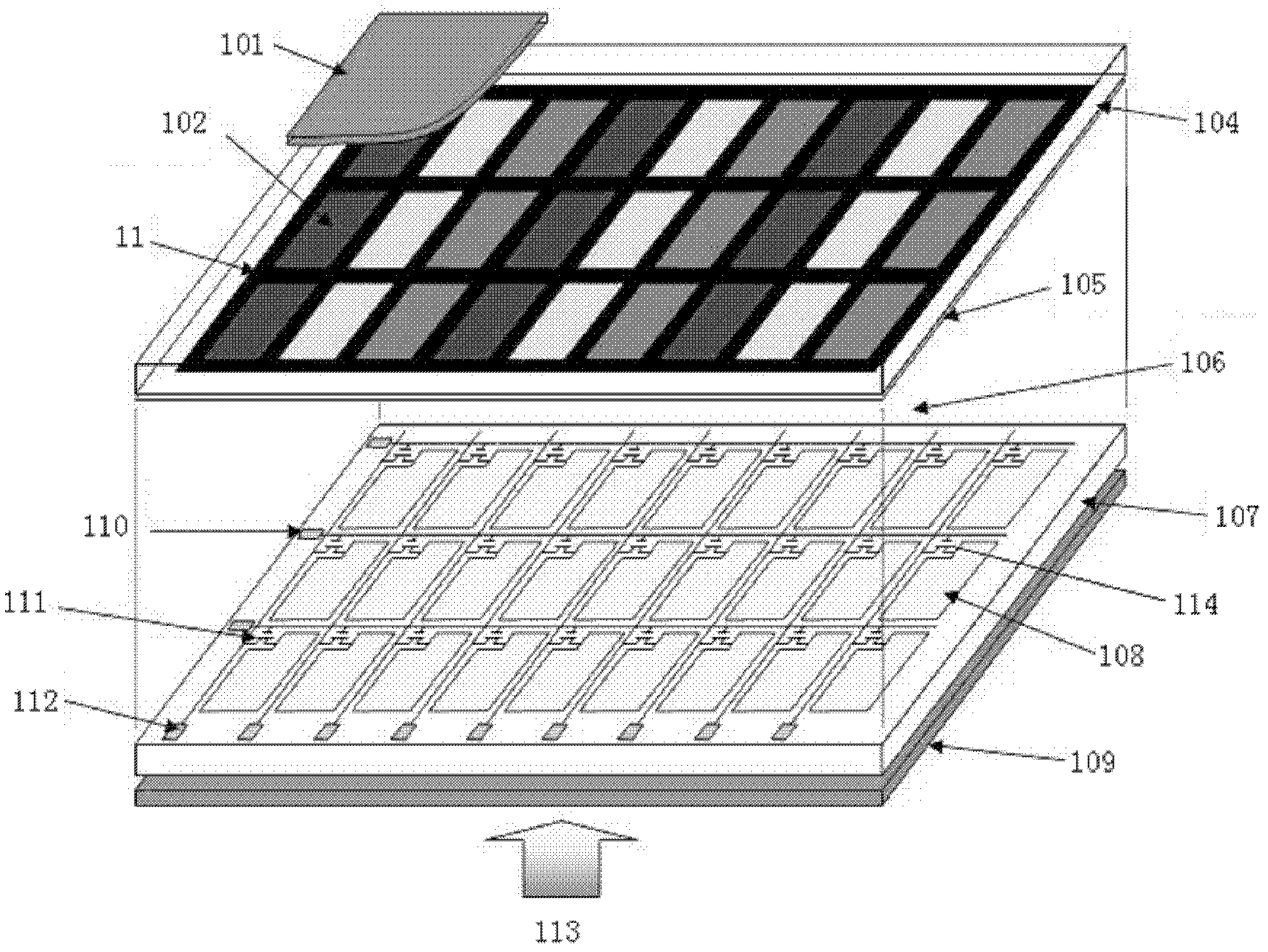
[0026] like Image 6 As shown, a step layer 18 is provided in the non-data line area coated with the sealant on the array substrate. Through the arrangement of this layer, the gap heights of the liquid crystal cells in the non-data line area and the data line area are different. Generally, the height of the non-data line area is set to be smaller than the height of the data line area, and the difference between the two heights should be much larger than the compression amount of the gold ball when the normal liquid crystal cell is thick. Through this method, the distance between the gold ball in the data line area and the common electrode on the color filter substrate and the data line layer is increased. The increased thickness of this part is composed of a sealing material, which is an epoxy resin material. The last is a reliable insulating material. In this way, the insulation is improved, that is, the electrostatic breakdown voltage of the double-layer insulating layer composed of the sealing glue layer and the insulating layer is increased, so that static electricity is not easy to pass through the gold ball and the data line. The insulating layer between them effectively prevents the short circuit between the data line at the coating of the sealant on the array substrate and the common electrode on the color filter substrate through the gold ball in the sealant, reducing the occurrence of display defects.

PUM

PropertyMeasurementUnit
Thickness5000.0 ~ 50000.0Å
tensileMPa
Particle sizePa
strength10

Description & Claims & Application Information

We can also present the details of the Description, Claims and Application information to help users get a comprehensive understanding of the technical details of the patent, such as background art, summary of invention, brief description of drawings, description of embodiments, and other original content. On the other hand, users can also determine the specific scope of protection of the technology through the list of claims; as well as understand the changes in the life cycle of the technology with the presentation of the patent timeline. Login to view more.

Similar technology patents

Classification and recommendation of technical efficacy words

  • Avoid short circuit
  • Improve insulation

Heat preservation covering agent

InactiveCN103042182AImprove insulationDelayed condensation rateThermal insulationPerlite
Owner:山国强
Why Eureka
Try Eureka