Organic light emitting diode (OLED) display driving chip and display

A technology of display driver and driver chip, applied in static indicators, instruments, electric solid devices, etc., can solve the problem that the driver chip cannot meet the needs of different placement positions.

Inactive Publication Date: 2011-11-23
SINO WEALTH ELECTRONICS
View PDF5 Cites 3 Cited by
  • Summary
  • Abstract
  • Description
  • Claims
  • Application Information

AI Technical Summary

Problems solved by technology

[0007] In view of this, the present invention provides an organic light-emitting diode (OLED) display driver chip to solve the technical problem that existing driver chips cannot meet the requirements of different placement positions

Method used


Image

  • Organic light emitting diode (OLED) display driving chip and display
  • Organic light emitting diode (OLED) display driving chip and display
  • Organic light emitting diode (OLED) display driving chip and display

Examples


Embodiment Construction

[0021] In order to make the above-mentioned features and advantages of the present invention more comprehensible, exemplary embodiments are given below together with accompanying drawings and described in detail as follows.

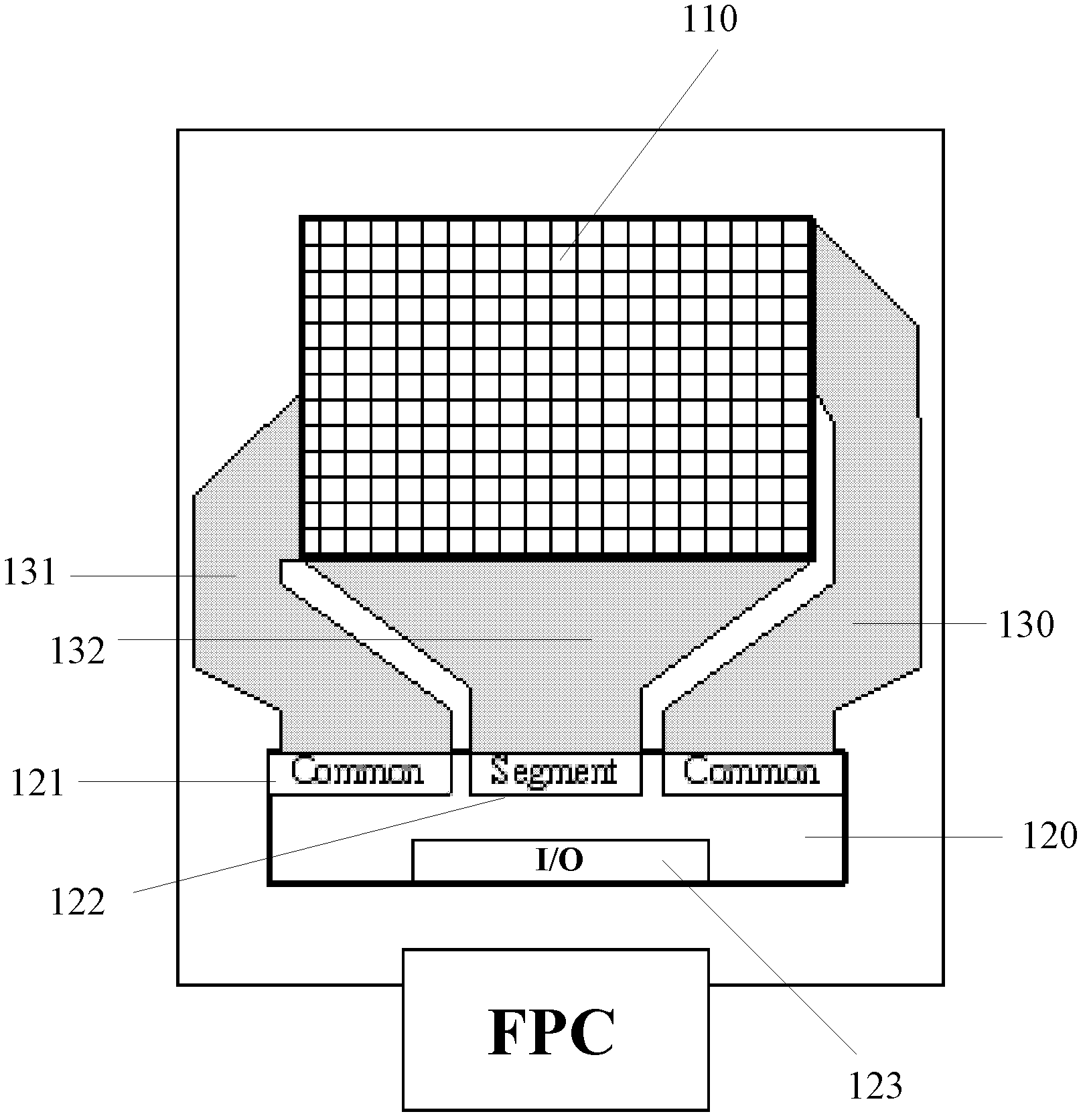
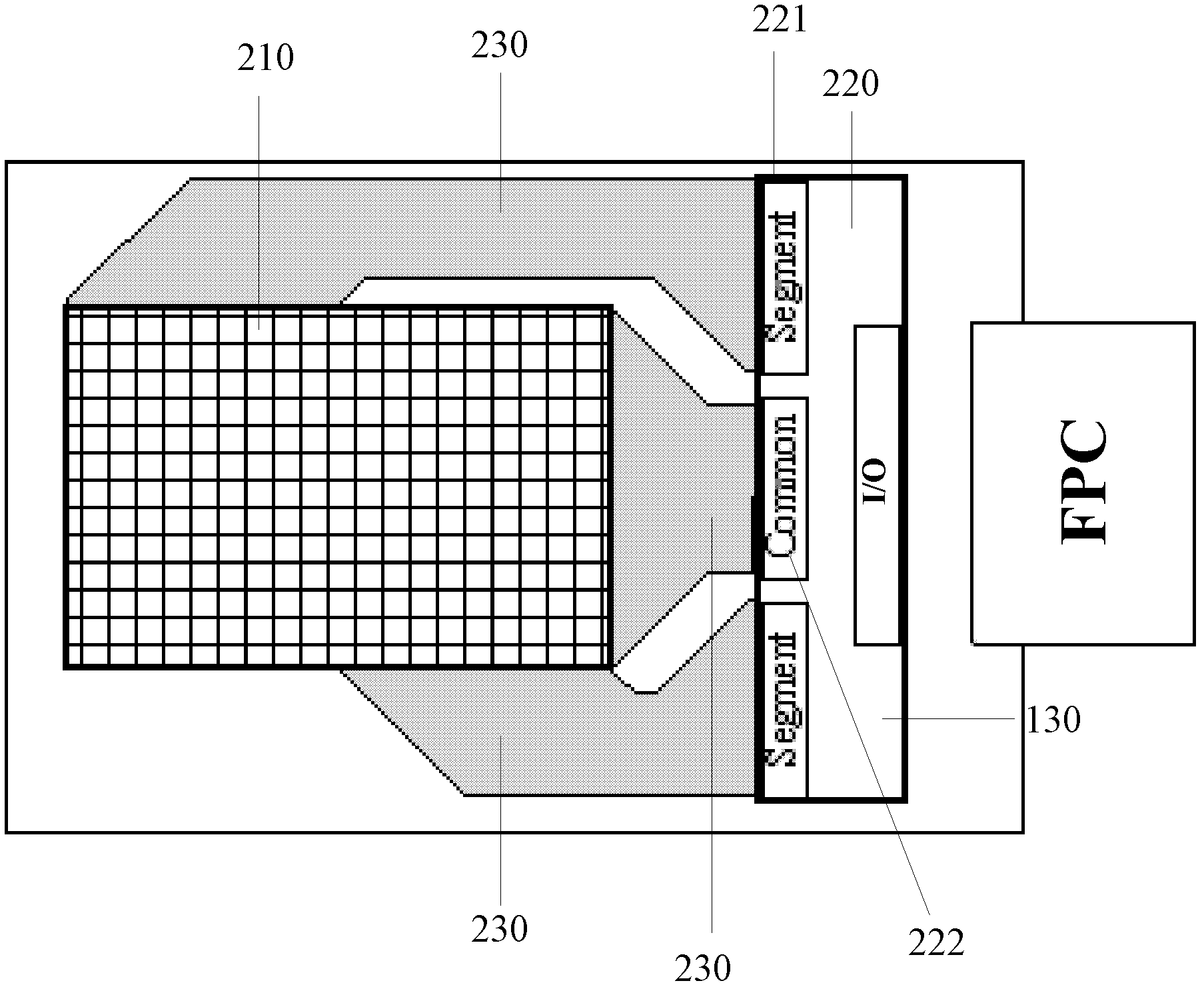
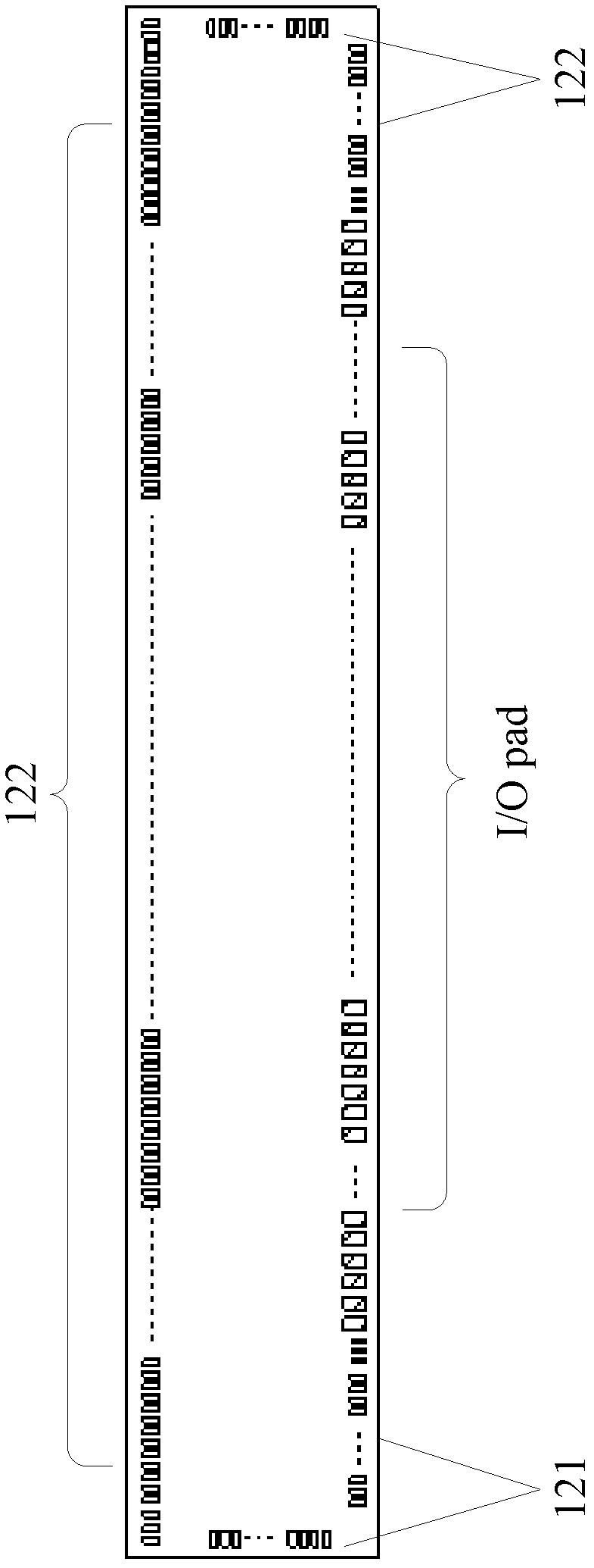
[0022] Considering the different layouts of organic light-emitting diode (OLED) display driver chips in practical applications, the present invention redesigns the chip port so that one chip can be applied to different layouts of OLED screens. Specifically, a set of common drive ports (Common ports) is added to the chip to select different ports for wiring in different placement methods, so that different placement requirements of OLED screens can be met without two chip designs. The specific structure and implementation principle are described through the following embodiments.

[0023] Please refer to Figure 5 , which is a schematic structural diagram of an OLED display driver chip provided by an embodiment of the present invention. As shown in the f...


PUM


Abstract

The invention discloses an organic light emitting diode (OLED) display driving chip, comprising a first common drive port, as well as a second common drive port and a third common drive port positioned at two sides of the first common drive port, and a first-segment drive port and a second-segment drive port which are arranged to space the first common drive port, the second common drive port and the third common drive port. Thus, a drive output port of the OLED display driving chip additionally provides a group of COM ports with repeat functions, which can be selected for use to meet different layout requirements, therefore, the layout requirements of different OLED screens can be met through the way that drive chips in the same type can use different COM ports.

Description

technical field [0001] The invention relates to the technical field of integrated circuits, in particular to an organic light-emitting diode (Organic Light-Emitting Diode, OLED) display driver chip and a display. Background technique [0002] Organic Light Emitting Diode (OLED) display technology is the most promising next-generation flat panel display technology after LCD technology. The basic structure of OLED is a thin and transparent indium tin oxide (ITO) with semiconducting properties, connected to the positive electrode of electricity, plus another metal cathode, wrapped into a sandwich structure. The whole structural layer includes: hole transport layer (HTL), light emitting layer (EL) and electron transport layer (ETL). When the power is supplied to an appropriate voltage, the positive holes and the negative charges will combine in the light-emitting layer to produce light, and the three primary colors of red, green and blue (RGB) are produced according to the form...

Claims


Application Information

Patent Timeline
IPC IPC(8): G09G3/32H01L27/32G09G3/3208
Inventor 计万里
Owner SINO WEALTH ELECTRONICS
Why Eureka
Try Eureka