Activation treatments in plating processes

A technology of activation treatment and electroplating process, applied in the direction of circuits, electrical components, electrical solid devices, etc., can solve the problems of reduced reliability, reduced performance, rough interface between electroplating layers, etc., to achieve the goal of reduced gaps, improved performance, and improved interface Effect

Inactive Publication Date: 2011-11-23
TAIWAN SEMICON MFG CO LTD
View PDF2 Cites 5 Cited by
  • Summary
  • Abstract
  • Description
  • Claims
  • Application Information

AI Technical Summary

Problems solved by technology

[0004] It was found that the interface between the electroplating layers is rough and voids are formed therein, which degrades the electro-migration (EM) performance of the bump, thus resulting in a decrease in its reliability

Method used


Image

  • Activation treatments in plating processes
  • Activation treatments in plating processes
  • Activation treatments in plating processes

Examples


Embodiment Construction

[0026] The making and using of embodiments of the invention are described in detail below. It should be understood that many inventive concepts provided by these embodiments can be widely applied to various specific fields. The specific embodiments described are by way of illustration only and are not intended to be limiting.

[0027] In one embodiment, a novel process for forming an integrated circuit is provided. Intermediate stages in the manufacture of this embodiment are shown. Various embodiments are discussed in this disclosure. In different drawings and embodiments, similar reference numerals will be used to refer to similar elements.

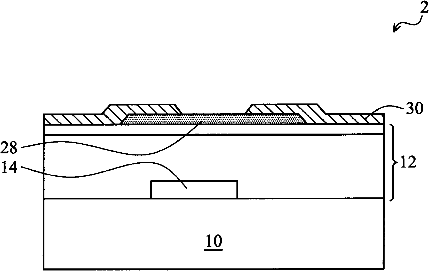
[0028] refer to figure 1 , a wafer 2 comprising a substrate 10 is provided. The substrate 10 may be a semiconductor substrate such as a bulk silicon substrate, but may also include other semiconductor materials such as silicon germanium, silicon carbide, gallium arsenide, and the like. Semiconductor devices 14 such as transistors...


PUM


Abstract

A method of forming a device includes performing a first plating process to form a first metallic feature, and performing an activation treatment to a surface of the first metallic feature in an activation treatment solution, wherein the activation treatment solution includes a treatment agent in de-ionized (DI) water. After the step of performing the activation treatment, performing a second plating process to form a second metallic feature and contacting the surface of the first metallic feature.

Description

technical field [0001] The invention relates to an integrated circuit, in particular to an electroplating process, and more to a process for forming bumps by the electroplating process. Background technique [0002] When forming a semiconductor chip, integrated circuit devices such as transistors are first formed on the surface of a semiconductor substrate in the semiconductor chip. An interconnection structure is then formed on the integrated circuit device. Bumps are formed on the surface of the semiconductor chip as contacts of integrated circuit devices. [0003] In a specific process for forming bumps, an under-bump metallurgy (UBM) is formed first, and then a bump is formed on the UBM. The formation of the UBM may include forming a copper seed layer, and forming a patterned mask on the copper seed layer, and a part of the copper seed layer is exposed through openings of the mask. An electroplating step is then performed on the exposed portion of the copper seed laye...

Claims


Application Information

Patent Timeline
Patent Type & Authority Applications(China)
IPC IPC(8): H01L21/60H01L23/00C25D7/12C25D5/54
CPCH01L2924/01074H01L2924/01006H01L21/288H01L2924/00013H01L2224/13139H01L2924/01327H01L2224/11424H01L2924/10329H01L2224/93H01L24/11H01L2924/01082H01L2224/05166H01L2224/05644H01L2924/01072H01L2224/0401H01L2224/05181H01L2224/11462H01L2224/13118H01L2924/01073H01L2924/01033H01L2224/05572H01L2224/11464H01L2924/01047H01L2224/05624H01L24/12H01L2924/01079H01L24/13H01L2224/13083H01L2224/11622H01L2924/01013H01L2924/01322C25D7/123H01L2924/014H01L24/03H01L2224/13155H01L2224/05639H01L2224/05647H01L2224/11901H01L2224/1181H01L2924/01032H01L2224/13147H01L2924/01029C25D7/12H01L2224/0345H01L24/05H01L2224/03831H01L2924/0103H01L2924/0002H01L2224/11H01L2224/13099H01L2224/13599H01L2224/05599H01L2224/05099H01L2224/29099H01L2224/29599H01L2224/05552H01L2924/14H01L2224/1308H01L2924/00H01L2224/1146
Inventor 林志伟郑明达何明哲刘重希
Owner TAIWAN SEMICON MFG CO LTD
Why Eureka
Try Eureka