Charge pump circuit

A charge pump and circuit technology, applied in the direction of conversion equipment without intermediate conversion to AC, can solve the problems of poor matching degree and small Vt operating voltage range, and achieve the reduction of mismatch degree, large operating voltage range, and charging current. The effect of discharge current matching

Inactive Publication Date: 2011-11-23
SHANGHAI HUAHONG GRACE SEMICON MFG CORP
View PDF9 Cites 15 Cited by
  • Summary
  • Abstract
  • Description
  • Claims
  • Application Information

AI Technical Summary

Problems solved by technology

[0007] In order to overcome the disadvantages of poor matching between charging current and discharging current in the above-mentioned prior art charge pump circuit and the small Vt operating voltage range caused by improving the matching degree, the main purpose of the present invention is to provide a charge pump circuit that can achieve The purpose of not only improving the matching degree but also ensuring that the Vt operating voltage has a large range

Method used


Image

  • Charge pump circuit
  • Charge pump circuit
  • Charge pump circuit

Examples


Embodiment Construction

[0025] The implementation of the present invention will be described below through specific examples and in conjunction with the accompanying drawings, and those skilled in the art can easily understand other advantages and effects of the present invention from the content disclosed in the specification. The present invention can also be implemented or applied through other different specific examples, and various modifications and changes can be made to the details in this specification based on different viewpoints and applications without departing from the spirit of the present invention.

[0026] Figure 6 It is a circuit structure diagram of a preferred embodiment of a charge pump circuit in the present invention. Such as Figure 6 As shown, a charge pump circuit of the present invention includes a charging and discharging circuit 601 , a current replicating circuit 602 and an operational amplifier circuit 603 .

[0027] The charging and discharging circuit 601 include...


PUM


Abstract

The invention discloses a charge pump circuit, which at least comprises a charging / discharging circuit, a current duplicating circuit and an operational amplifier circuit, wherein the charging / discharging circuit comprises a charging module and a discharging module; an intermediate node of the charging module and the discharging module is connected to one input end of an operational amplifier; the current duplicating circuit is used for duplicating a charging current as well as generating a reference voltage; an output end of the current duplicating circuit is connected to the other input end of the operational amplifier; the output end of the operational amplifier circuit is connected to a discharging circuit and an NMOS (N-channel Metal Oxide Semiconductor)in a duplicating circuit; the operational amplifier circuit is used for controlling a discharging current of the discharging module to be equal to an NMOS current of the duplicating circuit; and the NMOS current of the duplicating circuit is equal to a PMOS current forever. The charge pump circuit provided by the invention is used for achieving the purposes of reducing a mismatching degree of the charging current and the discharging current and ensuring a working voltage scope outputted by a charge pump to be wider.

Description

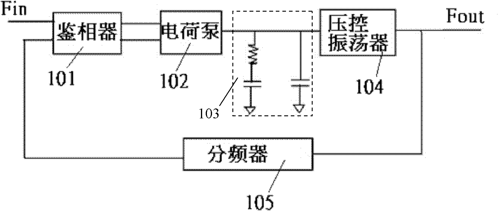
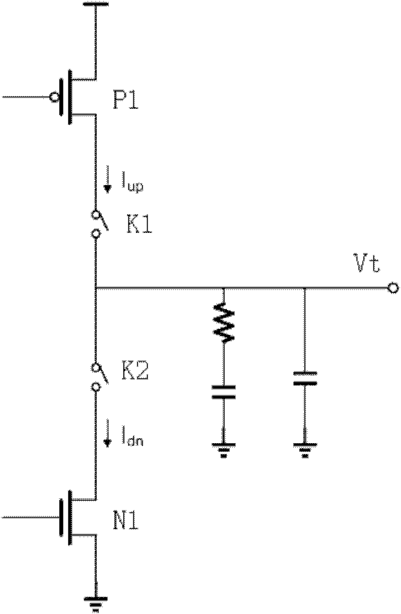
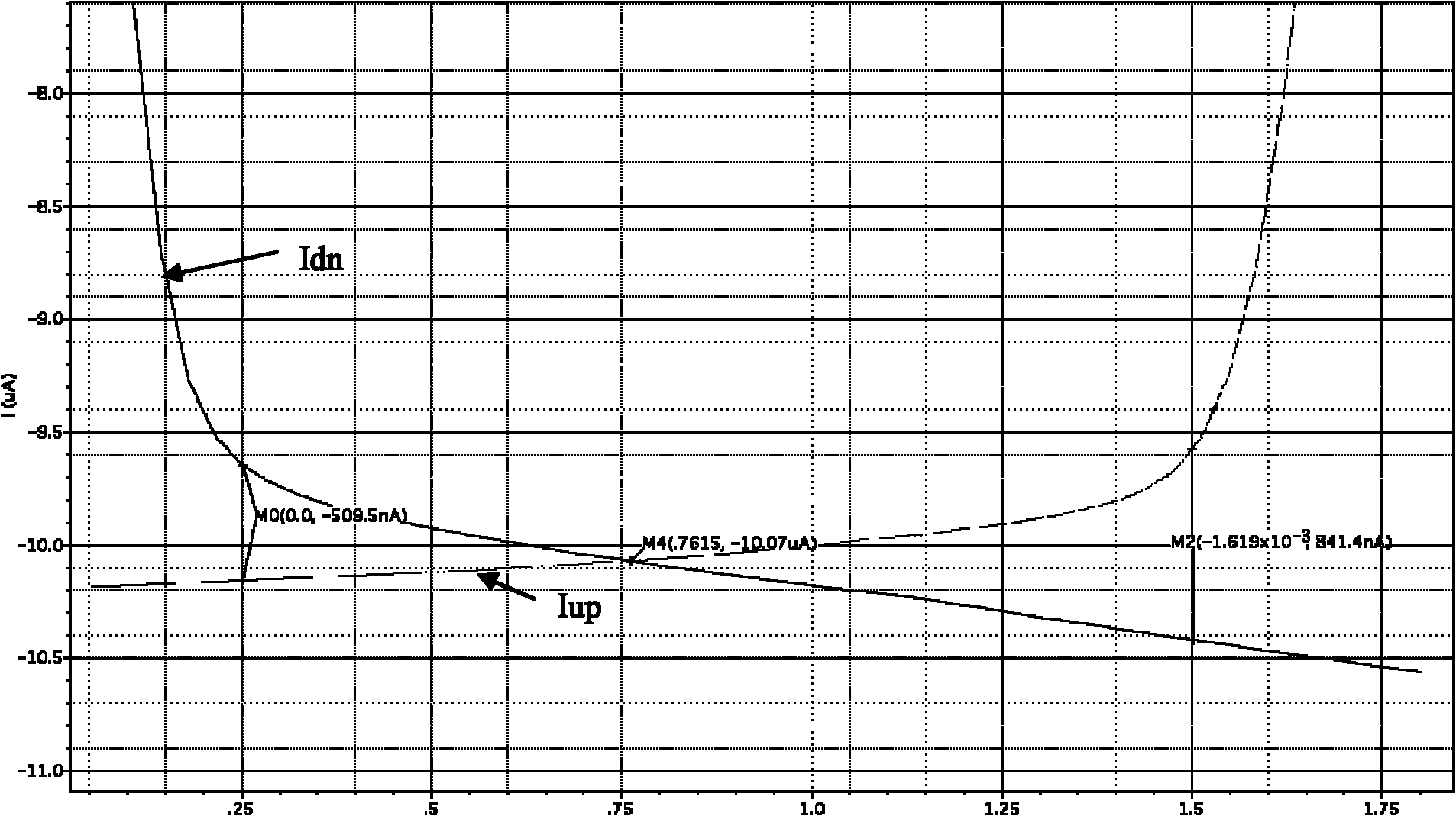
technical field [0001] The invention relates to a charge pump circuit, in particular to a charge pump circuit used in a phase-locked loop circuit. Background technique [0002] With the rapid development of integrated circuit technology, more and more attention has been paid to the phase-locked loop (PLL) circuit. At present, the phase-locked loop circuit plays an indispensable role in VLSI and system-on-chip. [0003] figure 1 It is a block diagram of an existing phase-locked loop circuit. Input the reference source Fin and output the oscillation signal Fout. The input reference source Fin and a feedback signal Fback are simultaneously input to the phase detector 101 for phase or frequency comparison, and the corresponding error signal is generated and sent to the charge pump 102, and the loop filter 103 accumulates the corresponding electric quantity to generate a voltage. Finally, the voltage-controlled oscillator 104 determines the operating point according to the vol...

Claims


Application Information

Patent Timeline
Patent Type & Authority Applications(China)
IPC IPC(8): H02M3/07
Inventor 吴冉青段新东彭进忠
Owner SHANGHAI HUAHONG GRACE SEMICON MFG CORP
Why Eureka
Try Eureka