Liquid crystal display substrate and method for manufacturing the same, liquid crystal panel and liquid crystal display

A liquid crystal display and manufacturing method technology, applied in the direction of instruments, nonlinear optics, optics, etc., can solve the problems of uneven thickness of the box in the sealing area, affecting the symmetry of the AC power supply, afterimages, etc., and achieve the effect of improving product quality

Active Publication Date: 2011-11-30
BEIJING BOE OPTOELECTRONCIS TECH CO LTD
View PDF4 Cites 46 Cited by
  • Summary
  • Abstract
  • Description
  • Claims
  • Application Information

AI Technical Summary

Problems solved by technology

[0006] Due to the uneven thickness of the sealant area around the liquid crystal display panel, and the inside of the sealant in the prior art is easy to separate ionic impurities, the above-mentioned ionic impurities will form residual DC electrons inside the liquid crystal, which will affect the AC flow of the impurity accumulation area. The symmetry of the power supply produces line afterimages

Method used


Image

  • Liquid crystal display substrate and method for manufacturing the same, liquid crystal panel and liquid crystal display
  • Liquid crystal display substrate and method for manufacturing the same, liquid crystal panel and liquid crystal display
  • Liquid crystal display substrate and method for manufacturing the same, liquid crystal panel and liquid crystal display

Examples


Embodiment Construction

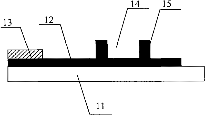
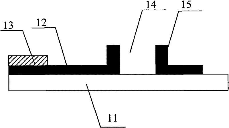
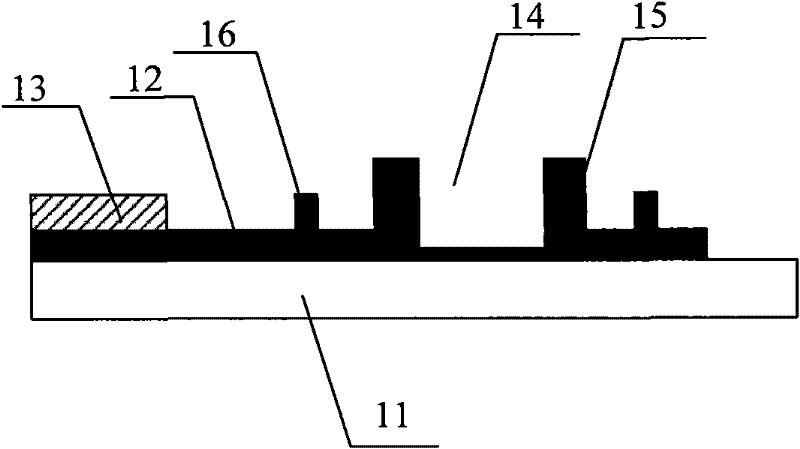
[0040] In order to make the purpose, technical solutions and advantages of the embodiments of the present invention clearer, the technical solutions in the embodiments of the present invention will be clearly and completely described below in conjunction with the drawings in the embodiments of the present invention. Obviously, the described embodiments It is a part of embodiments of the present invention, but not all embodiments. Based on the embodiments of the present invention, all other embodiments obtained by persons of ordinary skill in the art without creative efforts fall within the protection scope of the present invention.

[0041] In order to solve the defect in the prior art that ionic impurities are easily separated from the inside of the frame sealant, thereby affecting the symmetry of the AC power supply in the impurity accumulation area and causing line afterimages, an embodiment of the present invention provides a liquid crystal display substrate. The display s...


PUM

PropertyMeasurementUnit
heightaaaaaaaaaa
widthaaaaaaaaaa
heightaaaaaaaaaa

Abstract

The invention discloses a liquid crystal display substrate and a manufacturing method thereof, a liquid crystal display panel and a liquid crystal display, wherein the liquid crystal display substrate comprises an underlayment substrate and a film layer formed on the underlayment substrate; a box sealing glue groove is formed on the film layer in an edge region of the liquid crystal display substrate; and the box sealing glue groove is used for containing box sealing glue. The embodiment of the invention further provides a liquid crystal display panel, comprising an array substrate and a colour film substrate which are arranged in a folding way, wherein a liquid crystal layer is filled between the array substrate and the colour film substrate; the box sealing glue is filled in an edge region of the liquid crystal display panel; and at least one of the colour film substrate and the array substrate is adopted with the liquid crystal display substrate. The invention further provides a liquid crystal display. The liquid crystal display substrate and the liquid crystal display panel are capable of limiting the box sealing glue in a fixed region so as to effectively prevent the internal part of the box sealing glue from easily separating out ionic impurities, reduce the influence to the symmetrical characteristic of an alternating current power supply in an impurity gathering region and improve the product quality.

Description

technical field [0001] The invention relates to liquid crystal display technology, in particular to a liquid crystal display substrate and a manufacturing method thereof, a liquid crystal panel and a liquid crystal display. Background technique [0002] Liquid Crystal Display (hereinafter referred to as: LCD) has the characteristics of small size, low power consumption, and no radiation. It has made great progress in screen size and display quality, and it is rapidly replacing computer monitors and televisions CRT has become the mainstream product in the market. [0003] In liquid crystal displays, the sealant in the peripheral area of ​​the liquid crystal panel has a great influence on the product quality and is the basis for realizing high-quality liquid crystal display. The basic structure of the existing liquid crystal panel consists of polarizers, array substrates, color film substrates, and liquid crystal molecules. And so on. The inside of the frame sealant is usual...

Claims


Application Information

Patent Timeline
Patent Type & Authority Applications(China)
IPC IPC(8): G02F1/1339G02F1/1333
Inventor 马晓峰
Owner BEIJING BOE OPTOELECTRONCIS TECH CO LTD
Why Eureka
Try Eureka