Check patentability & draft patents in minutes with Patsnap Eureka AI!

Package substrate structure and manufacturing method thereof

A technology for packaging substrates and manufacturing methods, which is used in the manufacture of semiconductor/solid-state devices, electrical components, and electrical solid-state devices, etc., can solve the problems of small solder balls, solder bridges, and unstable tin amount in the printing solder paste step, and achieves Best reliability results, excellent coplanarity, increased bonding effect

Inactive Publication Date: 2011-11-30
NAN YA PRINTED CIRCUIT BOARD CORPORATION
View PDF3 Cites 5 Cited by
  • Summary
  • Abstract
  • Description
  • Claims
  • Application Information

AI Technical Summary

Problems solved by technology

However, due to the limitation of the distance between the open rings of the steel plate and the unevenness of the green paint coating on the substrate, the amount of tin added in the solder paste printing step will be unstable.
If the amount of tin is too much, it is easy to cause solder bridge phenomenon; if the amount of tin is too small, the volume of the solder ball will be too small, and the coplanarity of the conductive bump is insufficient, so that it cannot be electrically connected to the chip

Method used


Image

  • Package substrate structure and manufacturing method thereof
  • Package substrate structure and manufacturing method thereof
  • Package substrate structure and manufacturing method thereof

Examples


Embodiment Construction

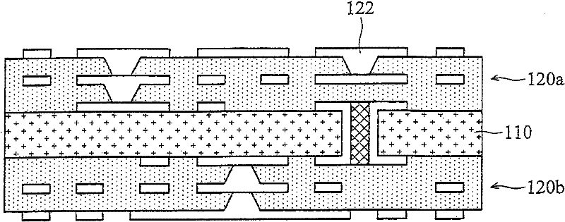
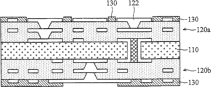
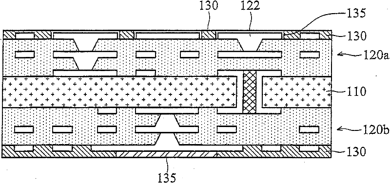
[0027] Hereinafter, each embodiment is described in detail and examples accompanied by accompanying drawings are used as a reference basis of the present invention. In the drawings or descriptions in the specification, the same reference numerals are used for similar or identical parts. And in the drawings, the shapes or thicknesses of the embodiments may be enlarged, and marked for simplicity or convenience. Furthermore, the parts of each element in the drawings will be described separately. It should be noted that the elements not shown or described in the drawings are forms known to those skilled in the art. In addition, the specific embodiment is only A specific method used in the present invention is disclosed, which is not intended to limit the present invention.

[0028] In view of this, the embodiment of the present invention provides a packaging substrate structure, in which the area between the circuits on the substrate is filled with solder resist insulating materi...


PUM


Abstract

The invention provides a packaging substrate structure and a manufacturing method thereof. The packaging substrate structure includes a substrate with a circuit layout; a build-up circuit structure is disposed on the substrate, wherein the build-up circuit structure has a plurality of ball planting pads; a first insulating layer is coated on the build-up circuit structure on the same height as the ball planting pads; an interface layer is disposed on the ball planting pads; a plurality of first solder balls are disposed on the interface layer of the ball planting pads, and the first solder balls are covered with a cladding layer; and a second insulating layer is disposed around the first solder balls, and has a raised portion rising along the side arc of the first solder balls; wherein the raised portion of the second insulating layer The raised portion is lower than the height of the first solder balls. The main advantage of the present invention is that after the previous step of coating the first insulating layer, it can provide a uniform and equal-height surface to be printed. Through the patterned etch step, the size of the ball pad can be precisely controlled.

Description

technical field [0001] The invention relates to a package substrate structure, in particular to a package substrate structure with a surface to be printed with uniform and equal height solder balls and a manufacturing method thereof. Background technique [0002] The development trend of electronic products has gradually evolved into light, thin, short, small, high-speed, high-frequency and multi-functional fields. In order to meet practical application requirements, semiconductor packaging technology has gradually evolved from a ball grid array (BGA for short) package and a flip chip carrier (FC for short) to a three-dimensional (3D) stacked structure. Alternatively, various packages are assembled and bonded by FC technology or wire bond (WB) technology to form a multi-functional structure. [0003] In the prior art, the solder ball array is implanted by printing solder paste on the substrate structure coated with a solder resist layer (such as green paint), followed by a ...

Claims


Application Information

Patent Timeline
Patent Type & Authority Applications(China)
IPC IPC(8): H01L23/498H01L21/48H01L21/60
CPCH01L2224/73204
Inventor 林贤杰
Owner NAN YA PRINTED CIRCUIT BOARD CORPORATION
Features
  • R&D
  • Intellectual Property
  • Life Sciences
  • Materials
  • Tech Scout
  • Unparalleled Data Quality
  • Higher Quality Content
  • 60% Fewer Hallucinations
Learn More