Micro-area optical damage test method and device
A technology of optical damage and testing methods, which is applied in measurement devices, material analysis by optical means, scientific instruments, etc., can solve problems such as inability to measure, and achieve the effect of overcoming large errors
- Summary
- Abstract
- Description
- Claims
- Application Information
AI Technical Summary
Problems solved by technology
Method used
Image
Examples
Embodiment Construction
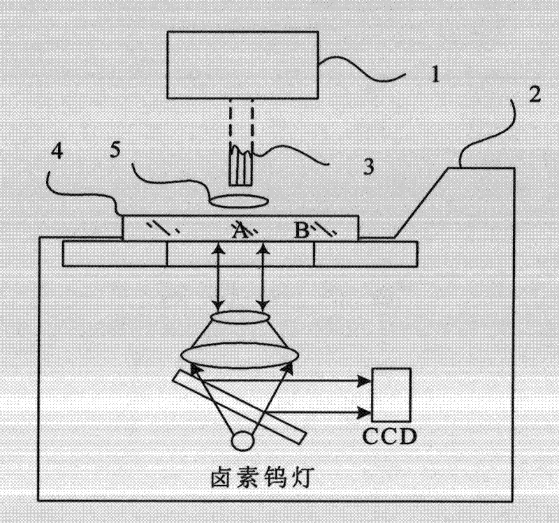
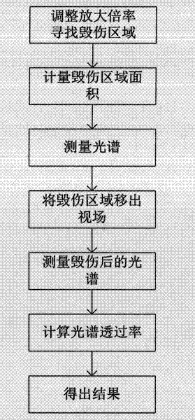
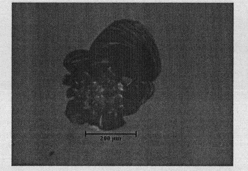
[0024] In the first step, take the K9 glass sample (4) and place it in the center of the field of view of the microscope (2), observe the size of the damaged area of the optical glass and its proportion in the field of view, and use the image processing function of the reading microscope (2) to measure the damage The size of the area, storing images such as figure 2 Shown.
[0025] In the second step, the optical fiber spectrometer (1) is used to measure the transmission spectrum of the sample before and after damage.
[0026] The third step is to calculate the spectral transmittance according to the spectral transmittance algorithm.
[0027] After measurement, the area of the damaged area is recorded as 548.2433, and the field of view area is 2202.1461
[0028] A D A = 0.248959
[0029] Use Origin software to calculate the transmission spectrum curve before and after damage, using the formula
[0030] ΔT(λ i )=T 0 (λ i )-T D (λ i )
[0031] E loss ( λ...
PUM
 Abstract
Description
Claims
Application Information


