Eureka AIR delivers breakthrough ideas for toughest innovation challenges, trusted by R&D personnel around the world.

Method and apparatus for producing silicon thin rods

A technology for thin silicon rods and equipment, which is used in the production of thin silicon rods and equipment, can solve problems such as unfavorable high resistance and complicated processes, and achieve the effects of increasing productivity and improving energy balance

Active Publication Date: 2011-12-21
光伏硅研究和生产有限责任公司
View PDF6 Cites 7 Cited by
  • Summary
  • Abstract
  • Description
  • Claims
  • Application Information

AI Technical Summary

Problems solved by technology

If these square cores are sawn from as-deposited high-purity polysilicon rods, they also have the disadvantageously high electrical resistance that begins to complicate the process during deposition

Method used


Image

  • Method and apparatus for producing silicon thin rods
  • Method and apparatus for producing silicon thin rods
  • Method and apparatus for producing silicon thin rods

Examples


Embodiment Construction

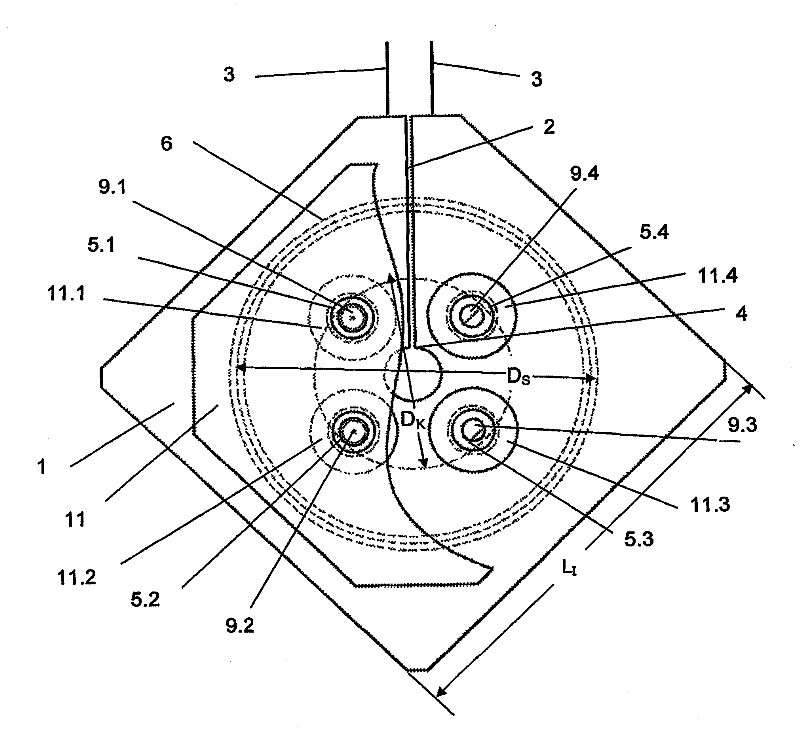
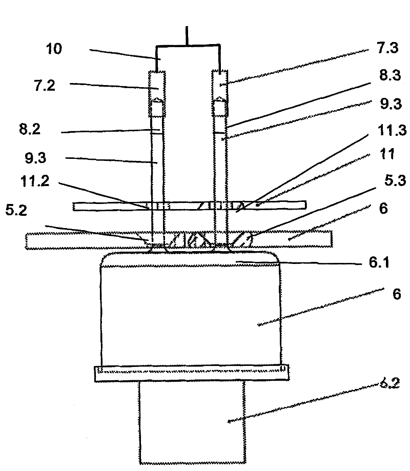
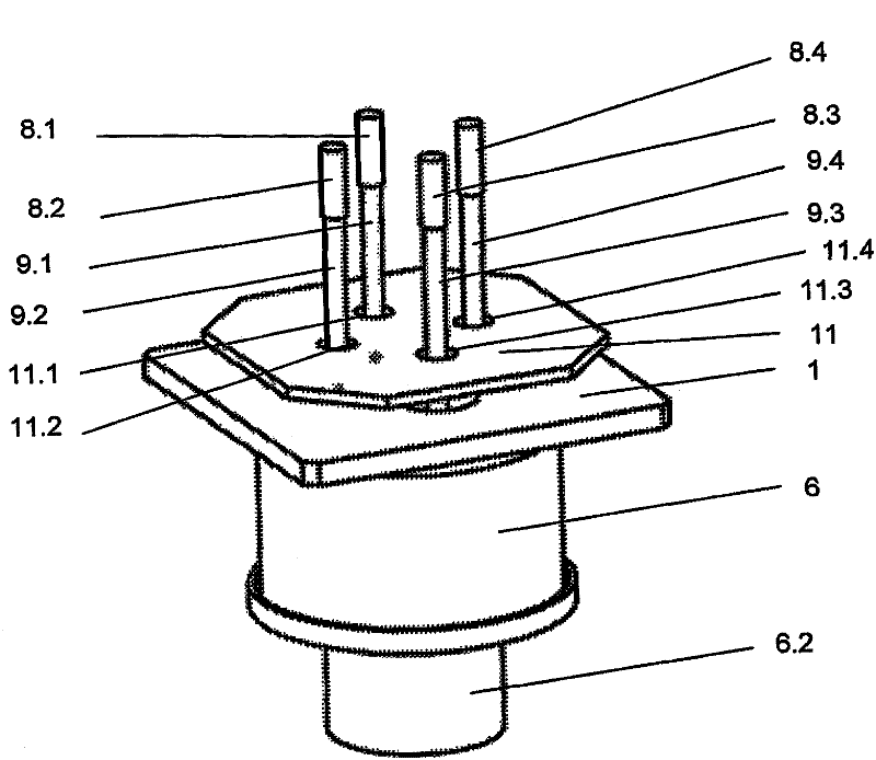
[0026] exist figure 1 A top view of an induction coil 1 embodied according to the invention is shown in . The induction coil 1 consists of a flat square metal disc. Edge length L of induction coil 1 I In the example it is 160mm and its thickness is 10mm. The induction coil 1 has in one of its diagonals a main slot 2 which opens into a central opening 4 in the middle of the induction coil 1 . A feeder 3 for an RF current is arranged laterally on the main slot 2 . So far, the configuration of the induction coil corresponds to the known prior art. According to the invention, the induction coil 1 has, in addition to the central opening 4 , further through-holes which serve as pulling openings 5.1, 5.2, 5.3, 5.4. Through the four pulling openings 5.1 , 5.2 , 5.3 , 5.4 the four thin silicon rods 9.1 , 9.2 , 9.3 , 9.4 can be pulled separately or simultaneously in selected examples. The pulling openings 5.1, 5.2, 5.3, 5.4 are distributed over the surface of the induction coil 1 ...


PUM

PropertyMeasurementUnit
diameteraaaaaaaaaa

Abstract

The invention relates to a method and to a device for producing thin silicon rods such as those used in the conventional Siemens process for precipitating silicon. Due to the strongly increasing demand for silicon for semiconductors and solar cells, the demand for thin silicon rods is also increasing. The method according to the invention fundamentally corresponds to the classical pedestal method. According to the invention, the induction coil (1) used comprises further draw openings (5.1, 5.2, 5.3, 5.4) about the central opening (4) having circumfluent current. A sufficiently uniform temperature profile is generated in the stock rod under the induction coil (1), such that the point of the stock rod melts and a melt pool forms (6.1) (6). One thin silicon rod (9.1, 9.2, 9.3, 9.4) each can be drawn upward out of the melt pool through the further draw openings in the induction coil. In contrast to the known prior art, no rod is drawn upward through the central opening having circumfluent current. The further additional draw openings are preferably disposed concentrically to the central opening and at a sufficient distance from the outer edge of the stock rod (6). The spacing thereof to each other is selected such that the growing thin silicon rods do not thermally influence each other too strongly, so that the individual thin silicon rods grow as uniformly as possible. The greater the diameter of the raw Si rod, the greater the diameter of the induction coil can be selected, and a correspondingly greater number of additional draw openings can be provided.

Description

technical field [0001] The present invention relates to a method and an apparatus for producing silicon thin rods as used for silicon deposition in the conventional Siemens process. Here, thin rods are arranged vertically in a reactor and heated to approximately 1100° C. by means of an electric current, so that silicon is pyrolytically deposited on the thin rods from a trichlorosilane-hydrogen mixture. This basic production process for polysilicon is essentially the same for the electronics industry as for the solar industry. Background technique [0002] As the demand for polycrystalline silicon as a raw material for silicon for semiconductors and as a raw material for solar cells has increased dramatically and continues to increase, the demand for silicon thin rods with a diameter of about 4-10 mm has correspondingly increased. The production of thin silicon rods is an unavoidable and also partly limiting component of the production of silicon rods by pyrolytic deposition...

Claims


Application Information

Patent Timeline
Patent Type & Authority Applications(China)
IPC IPC(8): C30B13/00C30B13/10C30B13/20C30B15/00C30B15/04
CPCC30B13/20C30B15/005C30B29/06Y10T117/1068Y10T117/1076Y10T117/1024Y10T117/1008Y10T117/1004Y10T117/1032Y10T117/10Y10T117/1088
Inventor H·里曼F-W·舒尔策J·菲舍尔M·伦纳
Owner 光伏硅研究和生产有限责任公司
Why Eureka
Eureka Blog
Learn More