Tunable flat absorbing material for electromagnetic waves

A technology for absorbing materials and electromagnetic waves, applied in layered products, chemical instruments and methods, metal layered products, etc., can solve problems such as complex development, and achieve the effects of adjustable absorption amplitude, various modulation methods, and large modulation amplitude.

Inactive Publication Date: 2012-01-04
UNIV OF ELECTRONICS SCI & TECH OF CHINA
View PDF7 Cites 24 Cited by
  • Summary
  • Abstract
  • Description
  • Claims
  • Application Information

AI Technical Summary

Problems solved by technology

The absorption material proposed in 2008 requires multi-step photolithography and alignment processes in the preparation process, and the development is relatively complicated, and its maximum absorption rate reaches 70%.
[0005] However, the existing electromagnetic wave absorbing materials based on Metamaterials are all passive. Once the preparation is completed, the absorption performance is determined.

Method used


Image

  • Tunable flat absorbing material for electromagnetic waves
  • Tunable flat absorbing material for electromagnetic waves
  • Tunable flat absorbing material for electromagnetic waves

Examples


Embodiment Construction

[0024] The preparation and implementation process of the tunable electromagnetic wave absorbing material provided by the present invention will be described in detail below by taking the microwave segment dual-frequency absorbing material and the temperature control method as examples:

[0025] Step 1: Structural design process: use the commercial software Microwave Studio CST to establish the structural model of the electromagnetic wave absorbing material based on metamaterials, optimize the structural size parameters so that the material works in the required frequency band, and obtain the best absorption effect at the required frequency point .

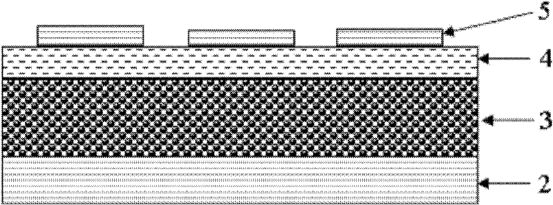
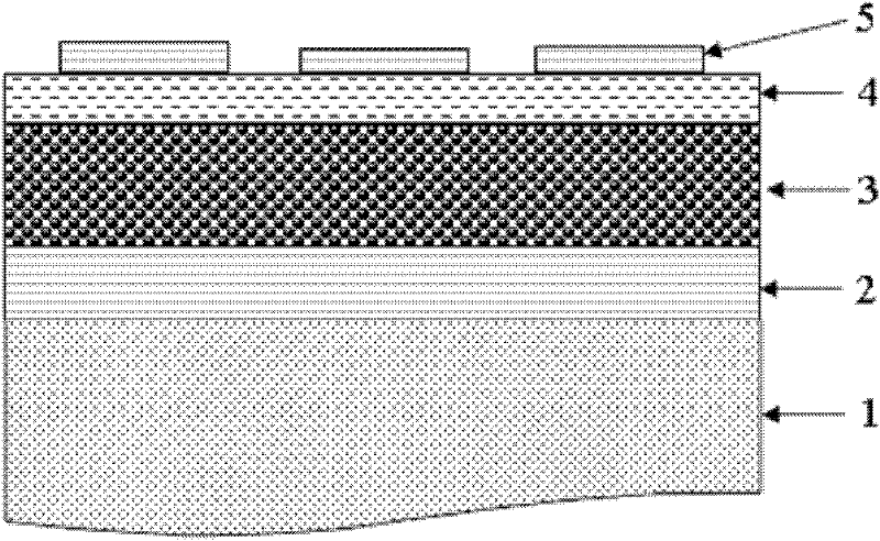
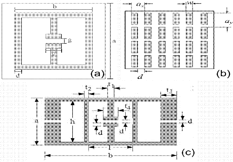
[0026] In the microwave frequency band, since the thickness of the dielectric layer can reach more than hundreds of microns, the dielectric layer can support the entire material at this time, so the substrate layer is no longer needed. image 3 (c) provides the structure of the single artificial unit adopted in this specific embodi...


PUM

PropertyMeasurementUnit
thicknessaaaaaaaaaa
thicknessaaaaaaaaaa

Abstract

The invention relates to a tunable flat absorbing material for electromagnetic waves and belongs to the technical field of electromagnetic functional material. The tunable flat absorbing material comprises a metal reflecting layer, a dielectric layer, a vanadium oxide phase-change material layer and a metamaterial layer; the dielectric layer is located between the metal reflecting layer and the vanadium oxide phase-change material layer; and the vanadium oxide phase-change material layer is located between the dielectric layer and the metamaterial layer. In the invention, a vanadium oxide phase-change film is inserted between the metamaterial layer and the dielectric layer of the three-layered electromagnetic wave absorbing material and used for controlling the absorption efficiency and the absorption frequency of the electromagnetic wave absorbing material by using the heat, electricity or light triggered phase-changing courses. The tunable flat absorbing material disclosed by the invention has simple structure and easiness in preparation and has the features of tuning absorption amplitude and absorption frequency, and the modulation depth of more than 70% can be achieved; the modulation manners are various and the modulation for absorbing terahertz wave can be realized by means of many manners such as heat or electricity or laser and the like; and the tunable flat absorbing material is applicable to electromagnetic protection, invisible technology, spectrum detection and thermal radiation and the like of the microwaves, terahertz waves and optical waves.

Description

technical field [0001] The invention belongs to the technical field of electromagnetic functional materials, and relates to electromagnetic wave absorbing materials, in particular to tunable electromagnetic wave planar absorbing materials. Background technique [0002] Metamaterial, or metamaterial, is an artificial electromagnetic coal quality composed of sub-wavelength artificial units arranged according to certain rules. Among them, since the size of the artificial unit is much smaller than the working wavelength, it is a material with uniform performance relative to the working wavelength. The advantage of metamaterials is that the electromagnetic properties of materials can be arbitrarily controlled by adjusting the structure, size and distribution of artificial units, so as to obtain a variety of novel properties. For example, metamaterials can be used to prepare left-handed materials, perfect lenses, and invisibility cloaks in the light band. And these characteristi...

Claims


Application Information

Patent Timeline
Patent Type & Authority Applications(China)
IPC IPC(8): B32B9/04B32B15/04B32B3/14
Inventor 文岐业张怀武杨青慧梁栋龙洋赵碧辉荆玉兰
Owner UNIV OF ELECTRONICS SCI & TECH OF CHINA
Why Eureka
Try Eureka