MEMS (micro electro mechanical system) apparatus and forming method thereof

A device and graphics technology, applied in the field of MEMS devices and MEMS technology, can solve the problems of high cost of ion implantation process, uniform distribution of doped ions, limitation of implantation depth, and complicated methods, so as to simplify the process and achieve different doping depths. Restricted, simple process effects

Active Publication Date: 2014-07-09
ADVANCED SEMICON MFG CO LTD
View PDF8 Cites 0 Cited by
  • Summary
  • Abstract
  • Description
  • Claims
  • Application Information

AI Technical Summary

Problems solved by technology

However, this method is relatively complicated, and the cost of the ion implantation process is very high, and the uniformity of the dopant ion distribution after implantation and the implantation depth are greatly restricted.

Method used


Image

  • MEMS (micro electro mechanical system) apparatus and forming method thereof
  • MEMS (micro electro mechanical system) apparatus and forming method thereof
  • MEMS (micro electro mechanical system) apparatus and forming method thereof

Examples


Embodiment Construction

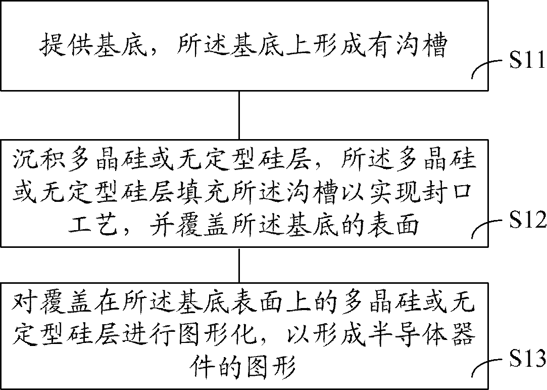
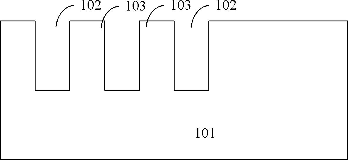
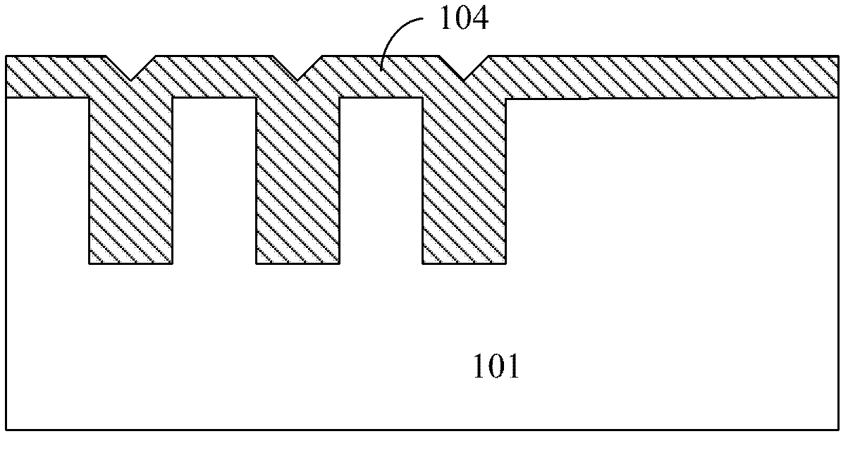
[0029] The MEMS devices in the prior art are often filled with materials such as silicon oxide, which has poor filling performance and is easily corroded by the external environment, resulting in potential reliability problems. In addition, in the prior art, the process of forming an integrated semiconductor device in a MEMS device is relatively complicated and costly.

[0030] In the MEMS device and its forming method according to the embodiment of the present invention, polysilicon or amorphous silicon is used to fill the groove on the substrate, and polysilicon or amorphous silicon has good filling properties, and has a good filling property when filling a trench with a high aspect ratio. performance, and polysilicon or amorphous silicon is more stable and reliable than conventional filling materials such as silicon oxide, which is conducive to improving the reliability of MEMS devices.

[0031] Further, in the forming method of the MEMS device of the embodiment of the pres...


PUM


Abstract

The invention provides an MEMS (micro electro mechanical system) apparatus and a forming method thereof. The forming method comprises the following steps: providing a substrate on which a groove is formed; depositing polycrystalline silicon or an amorphous silicon layer which is used for filling the groove to realize the sealing process and cover the surface of the substrate; patterning the polycrystalline silicon or amorphous silicon layer covered on the substrate surface so as to form a pattern of a semiconductor apparatus. The invention can improve the reliability of the filling, simplify the process flow and reduce the cost.

Description

technical field [0001] The invention relates to MEMS devices and MEMS process technology, in particular to a MEMS device and a forming method thereof. Background technique [0002] With the development of MEMS (Micro-Electro-Mechanical Systems) technology, MEMS devices have been widely used, such as micro-sensors, micro-motors and other micro-devices. Compared with traditional technologies, MEMS devices have the advantages of small size, low price, and high reliability. [0003] In the manufacturing process of MEMS devices, it is often necessary to form multiple trenches on the substrate, then etch the bottom of the trenches to form cavities, and finally fill the previously formed trenches with materials such as silicon oxide for sealing. On the one hand, filling materials such as silicon oxide have poor filling properties and are relatively easily corroded by various solutions and gases, which poses a potential threat to the reliability of the device; on the other hand, wh...

Claims


Application Information

Patent Timeline
Patent Type & Authority Patents(China)
IPC IPC(8): B81C1/00B81B1/00
Inventor 郑晨焱张挺
Owner ADVANCED SEMICON MFG CO LTD
Why Eureka
Try Eureka