Insulated gate bipolar transistor with floating buried layer

A bipolar transistor, insulated gate technology, applied in semiconductor devices, electrical components, circuits, etc., can solve problems such as difficulty in meeting the requirements of high-speed IGBT devices, low forward voltage drop, slow turn-off speed, etc. The effect of reverse safe working area, reducing forward voltage drop, and reducing turn-off time

Inactive Publication Date: 2012-01-04
UNIV OF ELECTRONICS SCI & TECH OF CHINA +1
View PDF5 Cites 13 Cited by
  • Summary
  • Abstract
  • Description
  • Claims
  • Application Information

AI Technical Summary

Benefits of technology

This innovation relates to an improved Insulated Gate Bipolar Transistors (IGBs) that has better performance at higher voltages than previous designs due to its use of multiple layers for added electrical properties such as increased carrier concentration near the surface of the channel material. These improvements make it possible to achieve greater efficiency without increasing resistance values.

Problems solved by technology

This patented technical problem addressed by this patents relates to improving insulating gate bioparallel tunnelingtransistors (IGTBFT), particularly at very fast speeds where traditional methods are limited due to their poor reverse voltage dropping characteristics or safety concerns associated with them.

Method used


Image

  • Insulated gate bipolar transistor with floating buried layer
  • Insulated gate bipolar transistor with floating buried layer
  • Insulated gate bipolar transistor with floating buried layer

Examples


Embodiment Construction

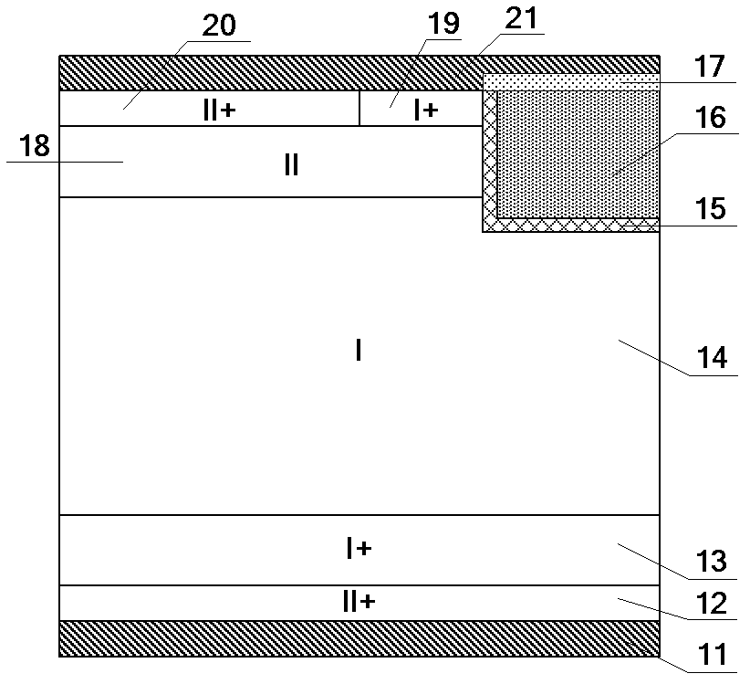
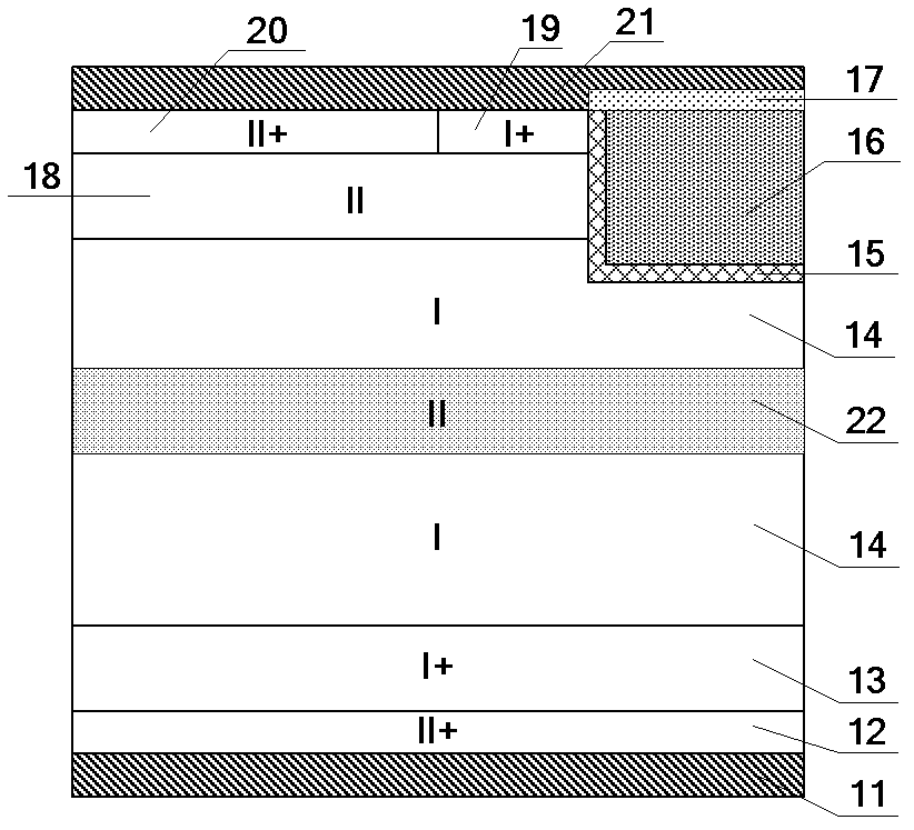
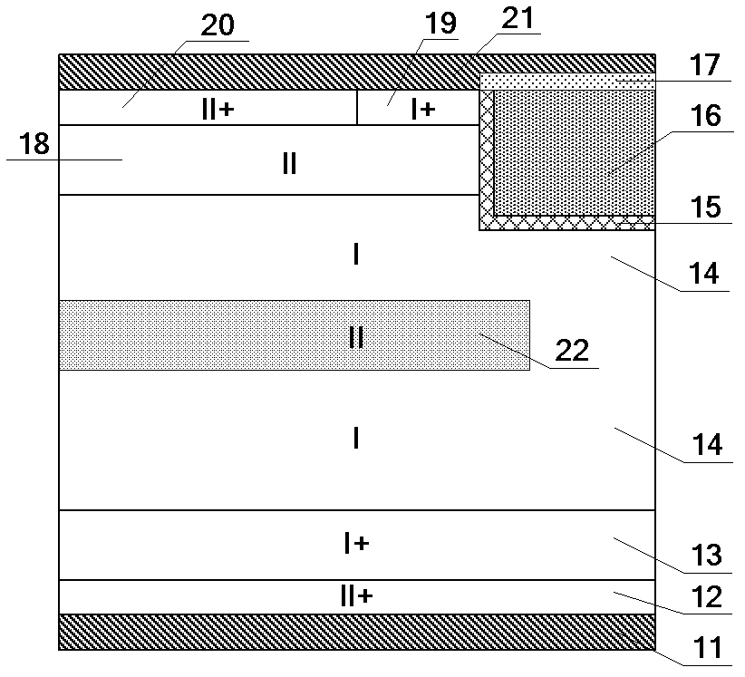
[0022] An insulated gate bipolar transistor with a floating buried layer, such as Figure 2 to Figure 7 As shown, there are one or more layers of continuous or discontinuous buried layers 21 of the second conductivity type in the drift region 14 of the first conductivity type of the IGBT.

[0023] In the above embodiment:

[0024] The buried layer 22 of the second conductivity type can be obtained through a two-step diffusion process on the substrate material of the first conductivity type before the traditional IGBT process starts. That is, before the start of the traditional IGBT process, a step-deep diffusion of impurities of the second conductivity type is performed on the substrate material of the first conductivity type, and then a shallow step of diffusion of impurities of the first conductivity type is performed to control the junction depth between the two diffusions. If it is poor, the buried layer 22 of the second conductivity type meeting the thickness and concent...


PUM


Abstract

The invention provides an insulated gate bipolar transistor (IGBT) with a floating buried layer, belonging to the power semiconductor device technology field. According to the invention, based on a traditional IGBT device structure, a drift region with a first conductive type is introduced with one or more layers of continuous or incontinuous second conductive type floating buried layers, through a modulation effect of introduced space charge and additional electric field of the second conductive type floating buried layer, new electric field peak is introduced into the drift region of the first conductive type, and with a same device drift region thickness, breakdown voltage of an IGBT device is substantially raised; with certain breakdown voltage, an IGBT device drift region thickness can be substantially reduced, thus forward conduction voltage drop and shutoff time of the device are substantially reduced. Simultaneously, with an effect of introduced space charge of the floating buried layer, avalanche breakdown in device shutoff can be inhibited, and dynamic breakdown voltage and reverse direction safety operation area of the IGBT device are improved.

Description


Claims


Application Information

Patent Timeline
Owner UNIV OF ELECTRONICS SCI & TECH OF CHINA
Why Eureka
Try Eureka