Active element, pixel structure, driving circuit and display panel

A technology of pixel structure and active components, which is applied in the fields of drive circuits, display panels, active components, and pixel structures, which can solve the problems of power consumption, increase of display panels, and increase of pixel structure load, etc., and achieve the effect of high aperture ratio

Active Publication Date: 2012-01-11
AU OPTRONICS CORP
View PDF4 Cites 8 Cited by
  • Summary
  • Abstract
  • Description
  • Claims
  • Application Information

AI Technical Summary

Problems solved by technology

However, since the overlapping of the capacitive electrode and the data line will increase the loading of the pixel structure, such a pixel structure will increase the power required for driving the display panel and consume more power.

Method used


Image

  • Active element, pixel structure, driving circuit and display panel
  • Active element, pixel structure, driving circuit and display panel
  • Active element, pixel structure, driving circuit and display panel

Examples


no. 1 example

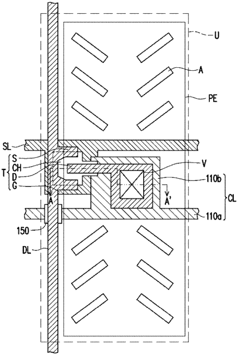
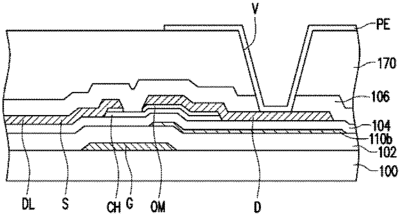
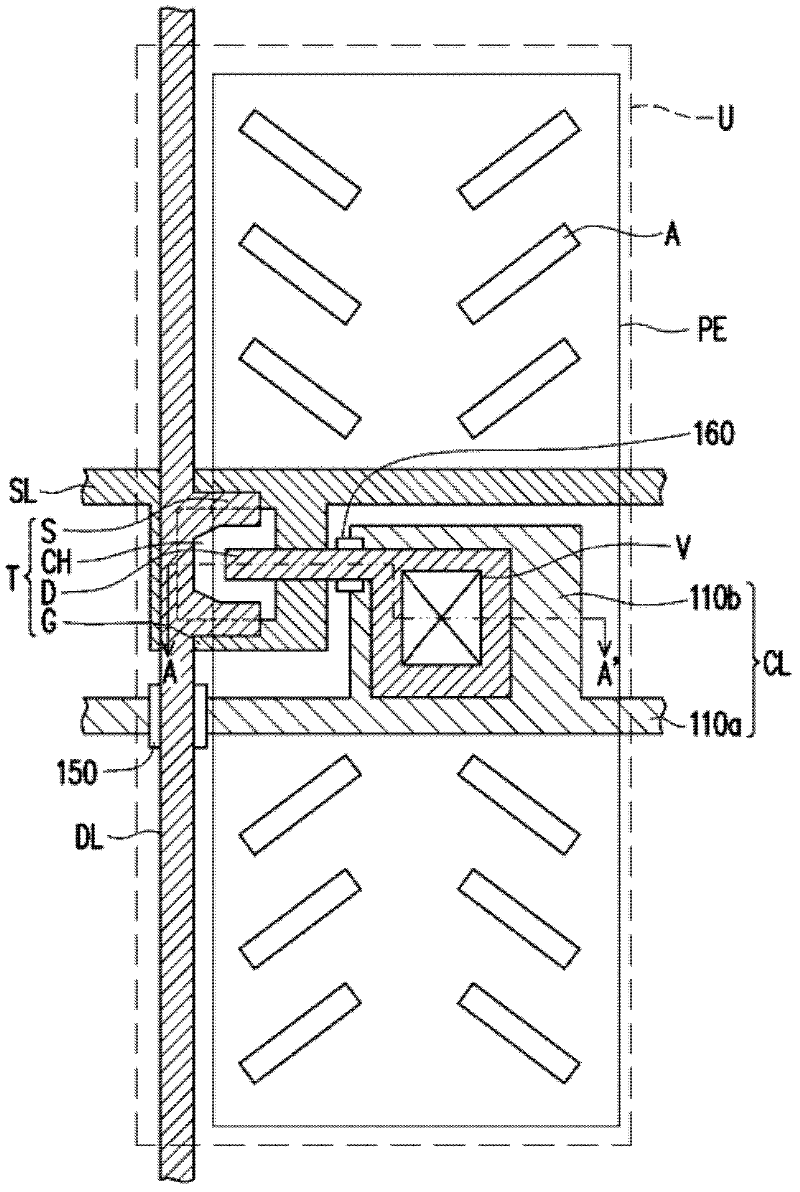
[0055] Figure 1A is a schematic top view of a pixel structure according to an embodiment of the present invention. Figure 1B yes Figure 1A Schematic cross-section along section line A-A'. Please also refer to Figure 1A as well as Figure 1B The pixel structure of this embodiment includes scan lines SL, data lines DL, active elements T, a first insulating layer 102 , pixel electrodes PE, capacitor electrodes CL and a second insulating layer 104 disposed on a substrate 100 .

[0056]The substrate 100 has a pixel area U, and one pixel structure is disposed in one pixel area U. The material of the substrate 100 can be glass, quartz, organic polymer, or opaque / reflective material (eg, conductive material, chip, ceramic, or other applicable materials), or other applicable materials. The scan lines SL and the data lines DL are disposed on the substrate 100 .

[0057] The scan lines SL and the data lines DL are arranged across each other (cross over). In other words, the exten...

no. 2 example

[0106] Figure 7 is a schematic top view of a display panel according to another embodiment of the present invention. Figure 8 yes Figure 7 A schematic cross-sectional view of a pixel structure and a driving circuit located in a pixel region in a display panel of FIG. Please refer to Figure 7 as well as Figure 8 , the display panel 400 of this embodiment has a display area 402 and a non-display area 404, and has a plurality of pixel areas U in the display area 402 of the display panel 400, and has at least one driving circuit in the non-display area 404 of the display panel 400 DR. The non-display area 404 substantially surrounds the display area 402 . The driving circuit DR can be located on one side, two sides, three sides or around the display area 402 . In this embodiment, the driving circuit DR is located on both sides of the display area 402 as an example for illustration, but the present invention is not limited thereto.

[0107] As mentioned above, the plura...

no. 3 example

[0120] Figure 10 is a schematic diagram of a driving circuit according to an embodiment of the present invention. Figure 11 yes Figure 10 A schematic cross-sectional view of one of the active components and one of the capacitors in the driving circuit of . Please refer to Figure 10 , the drive circuit of this embodiment, for example, can be applied to Figure 7 The driving circuit DR of the display panel is shown, and the driving circuit DR of this embodiment is a gate driving circuit as an example, but the present invention is not limited thereto. In this embodiment, the driving circuit includes a plurality of active elements M1 - M7 and a plurality of capacitors C1 - C2 . In addition, the scanning line Gn is electrically connected to the active elements M7 and M6 and the capacitor C2, the scanning lines Gn+1 and Gn-1 are electrically connected to the active elements M1 and M4 respectively, and the data line Vss is electrically connected to the active element M2. The...


PUM

PropertyMeasurementUnit
thicknessaaaaaaaaaa

Abstract

The invention provides an active element, a pixel structure, a driving circuit and a display panel. The pixel structure comprises a scanning cable, a data cable, the active element, a first insulation layer, a pixel electrode, a capacitor electrode and a second insulation layer. The active element comprises a grid, a gully, a source and a drain, wherein the scanning cable is electrically connected with the grid, and the source is electrically connected with the data cable. The first insulation layer is arranged between the grid and the gully. The pixel electrode is electrically connected with the drain. The capacitor electrode is arranged on the first insulation layer. The second insulation layer covers the first insulation layer and the capacitor electrode, and is arranged between the capacitor electrode and the drain.

Description

technical field [0001] The invention relates to an active element, a pixel structure, a driving circuit and a display panel with the active element. Background technique [0002] Generally speaking, a pixel structure of a liquid crystal display includes an active element and a pixel electrode. The active element is used as the switching element of the liquid crystal display unit. In order to control individual pixel structures, a specific pixel is usually selected through corresponding scan lines and data lines, and display data corresponding to the pixel is displayed by providing an appropriate operating voltage. In addition, the pixel structure also includes a storage capacitor, so that the pixel structure has a voltage holding function. That is, the storage capacitor can store the above-mentioned applied operating voltage to maintain the stability of the display picture of the pixel structure. [0003] In order to provide a storage capacitor in the pixel structure, it ...

Claims


Application Information

Patent Timeline
Patent Type & Authority Applications(China)
IPC IPC(8): G02F1/1362G02F1/1368G02F1/133G02F1/167H01L27/02
Inventor 林志宏蔡五柳魏全生张哲嘉刘圣超陈昱丞李怡慧陈茂松
Owner AU OPTRONICS CORP
Why Eureka
Try Eureka