Array baseplate and manufacturing method thereof as well as display panel using same

A technology of an array substrate and a manufacturing method, which is applied in the field of flat panel display, can solve the problems of lack of function of a single data line, dark lines of liquid crystal display, and high production cost, achieve good display effect, prevent display defects, and improve the effect of yield rate

Inactive Publication Date: 2012-01-11
SHENZHEN LAIBAO HI TECH
View PDF8 Cites 6 Cited by
  • Summary
  • Abstract
  • Description
  • Claims
  • Application Information

AI Technical Summary

Problems solved by technology

There is also a step difference between the part of the data lines arranged on the gate and the gate insulating layer and the part of the data lines only arranged on the gate insulating layer. Loss of functionality in a single data line, causing "dark lines" on the LCD
[0006] In addition, in a liquid crystal display, an organic layer needs to be provided to prevent short-circuiting between the electrode layer and the data line or gate line. , high production cost

Method used


Image

  • Array baseplate and manufacturing method thereof as well as display panel using same
  • Array baseplate and manufacturing method thereof as well as display panel using same
  • Array baseplate and manufacturing method thereof as well as display panel using same

Examples


Embodiment Construction

[0040] In order to illustrate the array substrate provided by the present invention, its manufacturing method, and the display panel using the array substrate, the following will be described in detail in conjunction with the accompanying drawings.

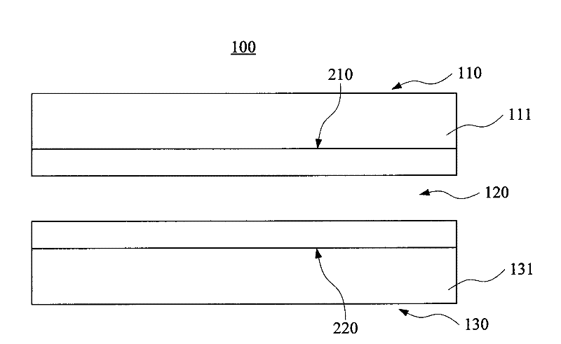
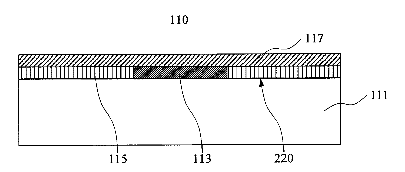
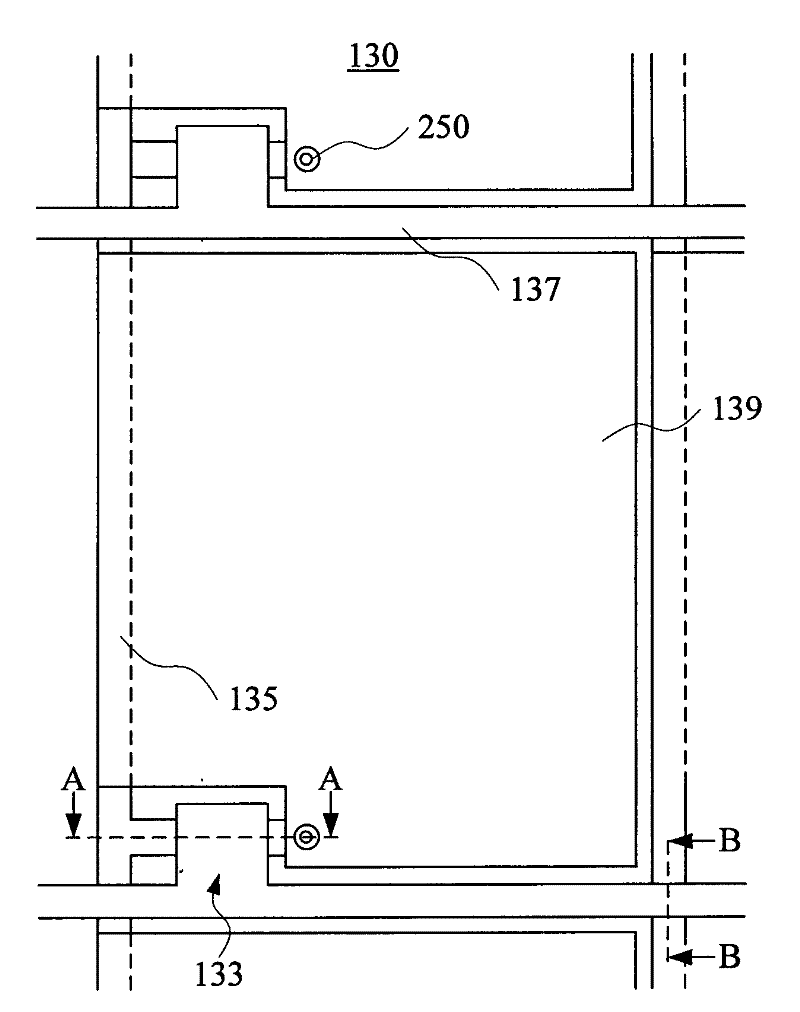
[0041] see figure 1 , which is a schematic diagram and a cross-sectional schematic diagram of a display panel according to a preferred embodiment of the present invention. The display panel 100 includes a color filter substrate 110 , a functional layer 120 and an array substrate 130 . The color filter substrate 110 is disposed opposite to the array substrate 130 , and there is a gap between the color filter substrate 110 and the array substrate 130 for accommodating the functional layer 120 . In this embodiment, the functional layer 120 is a liquid crystal layer. The color filter substrate 110 includes a first transparent substrate 111 having a first surface 210, and the array substrate 130 includes a second transparent substrat...


PUM


Abstract

The invention relates to the technical field of flat-plate display, in particular to an array baseplate, which comprises a second transparent substrate, a plurality of thin-film transistors and a plurality of data wires, wherein the second transparent substrate is provided with a third surface for forming a plurality of receiving spaces, and the thin-film transistors and the data wires are formed on the second transparent substrate; and each thin-film transistor comprises a source electrode and a drain electrode, and the source electrodes of the thin-film transistors positioned on the same column are connected with a same data wire and are received in the receiving spaces together with the drain electrodes of the thin-film transistors. In addition, the invention also provides a manufacturing method of the array baseplate and a display panel using the array baseplate.

Description

technical field [0001] The present invention relates to the field of flat panel display technology, in particular to an array substrate, a manufacturing method thereof, and a display panel using the array substrate. Background technique [0002] Due to its advantages such as low power consumption and small size, liquid crystal displays have widely replaced CRT displays and become the mainstream displays today. [0003] As we all know, a liquid crystal display mainly includes a color filter substrate, a liquid crystal layer, and an array substrate. The color filter substrate is arranged opposite to the array substrate, and the liquid crystal layer is arranged between the color filter substrate and the array substrate. The array substrate includes a plurality of glass substrates, gate lines, data lines, thin film transistor structures, gate insulating layers, passivation layers, organic layers, pixel electrode layers and the like. The manufacturing process of the liquid crys...

Claims


Application Information

Patent Timeline
Patent Type & Authority Applications(China)
IPC IPC(8): H01L27/02H01L21/77G02F1/1362G02F1/1368
Inventor 王士敏朱泽力商陆平李绍宗
Owner SHENZHEN LAIBAO HI TECH
Why Eureka
Try Eureka