
Lead wire structure and displaying panel possessing the lead wire structure

A technology for display panels and leads, applied in nonlinear optics, optics, instruments, etc.

Inactive Publication Date: 2012-01-18
AU OPTRONICS CORP
View PDF5 Cites 8 Cited by
  • Summary
  • Abstract
  • Description
  • Claims
  • Application Information

AI Technical Summary

Problems solved by technology

The pixel array is located in the display area
The drive unit is located in the non-display area

Method used


Image

  • Lead wire structure and displaying panel possessing the lead wire structure
  • Lead wire structure and displaying panel possessing the lead wire structure
  • Lead wire structure and displaying panel possessing the lead wire structure

Examples


Embodiment Construction

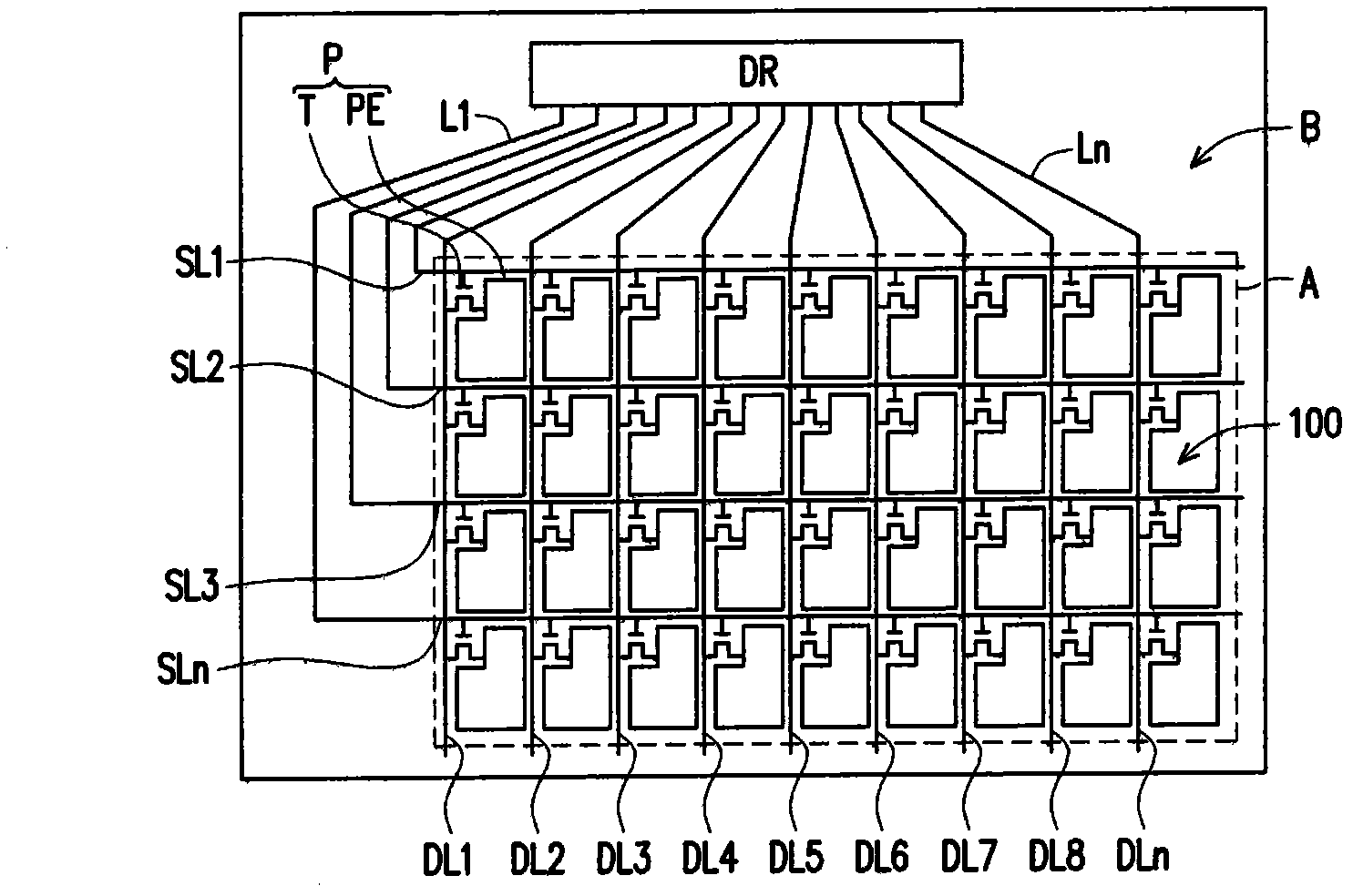
[0021] figure 1 is a schematic top view of a display panel according to an embodiment of the present invention. figure 2 yes figure 1 A schematic diagram of the lead structure of the display panel. Please also refer to figure 1 as well as figure 2 , the display panel of this embodiment includes a display area A and a non-display area B around the display area A. The display panel includes a pixel array 100, at least one driving device DR and a plurality of leads L1-Ln.

[0022] The pixel array 100 is located in the display area A. As shown in FIG. According to this embodiment, the pixel array 100 includes a plurality of scan lines SL1 -SLn, a plurality of data lines DL1 -DLn, and a plurality of pixel structures P. Referring to FIG.

[0023] The scan lines SL1 ˜SLn and the data lines DL1 ˜DLn are disposed across each other, and an insulating layer is interposed between the scan lines SL1 ˜SLn and the data lines DL1 ˜DLn. In other words, the extending direction of the s...


PUM


Abstract

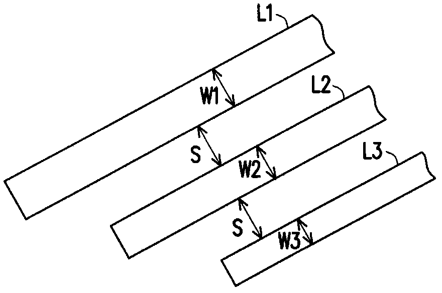
The invention discloses a lead wire structure and a displaying panel possessing the lead wire structure, comprising a displaying zone and a non-displaying zone. The displaying panel comprises a pixel array, at least one driving device and a plurality of lead wires. The pixel array is located in the displaying zone, and the driving device and the lead wires are located in the non-displaying zone; the lead wires are in electrical connections with the pixel array and the driving device, and are arranged as a fan-shaped structure between the pixel array and the driving device. Especially, the wire distance P<n-1> between the No.(n-1) lead wire and the No. n lead wire is equal to (W<n-1>+S), wherein, the n is a positive integer greater than 1, the W<n-1> represents the wire width of the No.(n-1) lead wire, and the S represents the clearance of adjacent lead wires; wherein, the wire distances P<1> to P<n-1> of the lead wires in the fan-shaped structure are not completely equal.

Description

technical field [0001] The invention relates to a lead structure and a display panel with the lead structure. Background technique [0002] Generally speaking, a liquid crystal display panel in a liquid crystal display is composed of a pixel array substrate, a color filter array substrate and a liquid crystal layer sandwiched between the two substrates. In the pixel array substrate, lead wires are also provided in the non-display area to electrically connect the pixel array and the driving chip. [0003] Generally, in order to match the contacts of the driver chip, the wires disposed between the pixel array and the driver chip are arranged in a fan-out structure. However, the lead wires located at the edge area of ​​the fan-shaped structure and the lead wires located at the middle area of ​​the fan-shaped structure have different lengths, so that the impedances of these lead wires are inconsistent. As a result, there will be obvious delay differences between the signal tra...

Claims


Application Information

Patent Timeline
Patent Type & Authority Applications(China)
IPC IPC(8): G02F1/13H01L27/02
CPCG02F1/13452H01L27/02
Inventor 郑耕全傅建豪
Owner AU OPTRONICS CORP
Learn More