Unlock instant, AI-driven research and patent intelligence for your innovation.
Schottky barrier metal oxide semiconductor (MOS) transistor and preparation method thereof
What is Al technical title?
Al technical title is built by PatSnap Al team. It summarizes the technical point description of the patent document.
A technology of MOS transistor and Schottky potential, applied in the field of Schottky barrier MOS transistor and its preparation, can solve the problems of large on-current, large on-current of devices, etc., so as to improve the on-current and the on-state. current, the effect of increasing the on-state current
Active Publication Date: 2013-07-31
SEMICONDUCTOR MANUFACTURING INTERNATIONAL (BEIJING) CORP +1
View PDF2 Cites 0 Cited by
Summary
Abstract
Description
Claims
Application Information
AI Technical Summary
This helps you quickly interpret patents by identifying the three key elements:
Problems solved by technology
Method used
Benefits of technology
Problems solved by technology
First of all, since the on-state current mainly comes from the tunneling of the source carrier, the on-state current is limited, and the small on-state current becomes one of the main reasons for limiting the application of SB-MOSFET; secondly, SB-MOSFET has a serious bipolar effect, that is, when the gate is reverse-biased, the device will also generate a large conduction current, so that the gate will appear when a certain forward and reverse bias is applied. Large conduction current
Method used
Image
Click on the blue label to locate the original text in one second.
Reading with bidirectional positioning of images and text.
Examples
Embodiment 1
[0044] Adopt the following method to prepare the MOS transistor of the present invention:
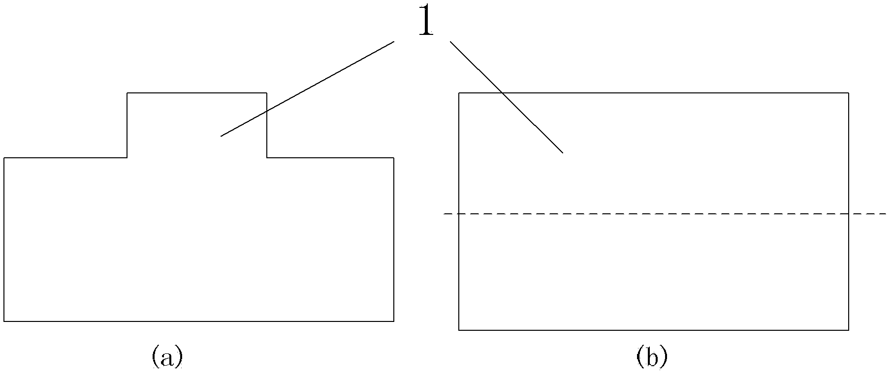
[0045] (1) On the bulk silicon wafer silicon substrate 1 with the crystal orientation of (100), the shallow trench isolation technology is used to fabricate the active region isolation layer, and the doping concentration of the substrate is N-type lightly doped; then, a step pattern is formed by photolithography , etch a step structure, the step height is about 500nm, such as figure 1 (a), 1(b);
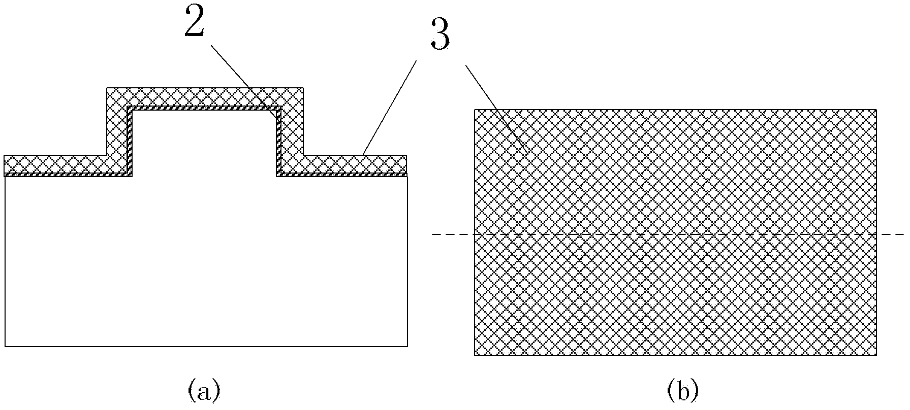
[0046] (2) thermally grow the gate dielectric layer, and then deposit the gate electrode layer, the gate dielectric layer is SiO 2 , the thickness is 1-5nm, the gate electrode layer is a highly doped polysilicon layer, the thickness is about 200nm, such as figure 2 (a), as shown in 2(b);
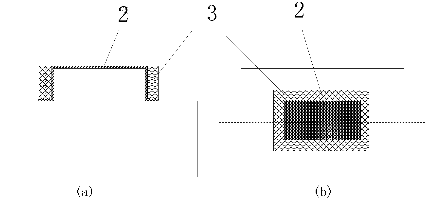
[0047] (3) The ring-shaped gate electrode 3 is formed by using the sidewall process, and the thickness of the gate electrode is about 200nm, such as image 3 (a), 3(b);
[0048] (4) Deposit the side wa...
Embodiment 2
[0053] As in Example 1, the difference is:
[0054] The step height in step (1) is about 200nm;
[0055] The thickness of the gate electrode in steps (2) and (3) is about 100nm;
[0056] The thickness of the sidewall in steps (4) and (5) is about 50nm;
[0057] ●The sputtered metal in step (6) is a metal with a smaller hole Schottky barrier, such as Pt.
Embodiment 3
[0059] As in Example 1, the difference is:
[0060] The substrate doping in step (1) is P-type lightly doped;
[0061] ●The sputtered metal in step (6) is a metal with a small electronic Schottky barrier, such as rare earth metal Er or Yb.
PUM
Abstract
The invention discloses a Schottky barrier metal oxide semiconductor (MOS) transistor, which comprises a ring-shaped gate electrode (3), a ring-shaped gate dielectric layer (2), a ring-shaped gate electrode side wall (4), a semiconductor substrate, a source region (5) and a ring-shaped drain region (6). The Schottky barrier MOS transistor is characterized in that: the semiconductor substrate is provided with a convex step structure; the source region is positioned on a high plane of a convex step; the ring-shaped drain region surrounds the convex step and is positioned on a low plane; the gate dielectric layer and the gate electrode are positioned at a corner of the convex step, surrounds the step and is raised into a ring shape; and the gate electrode side wall is ring-shaped, surrounds on the outer side of the gate electrode and has a certain thickness to serve as a shelter to form an underlap structure of a drain terminal. The Schottky barrier MOS transistor adopts a step structurecombining a ring-shaped gate structure and an asymmetric source / drain structure, so on the basis of inheriting advantages of traditional SB-MOSFET, the on-state conduction current is improved, a dipolar effect is inhibited, and the process is simplified.
Description
technical field [0001] The invention belongs to the field of field effect transistor logic devices and circuits in CMOS ultra-large integrated circuits (ULSI), and specifically relates to a Schottky barrier MOS transistor combined with a step structure, a ring gate structure and an asymmetric source / drain structure and its preparation method. Background technique [0002] As early as the late 1960s, Lepselter and Sze proposed the Schottky Barrier MOSFET (Schottky Barrier MOSFET) structure. The source and drain are replaced with metal or silicide for traditional doping, and the direct tunneling barrier of carriers at the source end is used to achieve conduction. As the size of metal-oxide-silicon field-effect transistors (MOSFETs) continues to shrink, short-channel effects are increasingly affecting the devices. For traditional MOS field effect transistors, in order to suppress the short-channel effect, ultra-shallow junctions and abruptly doped source / drain regions must be...
Claims
Application Information
Patent Timeline
Application Date:The date an application was filed.
Publication Date:The date a patent or application was officially published.
First Publication Date:The earliest publication date of a patent with the same application number.
Issue Date:Publication date of the patent grant document.
PCT Entry Date:The Entry date of PCT National Phase.
Estimated Expiry Date:The statutory expiry date of a patent right according to the Patent Law, and it is the longest term of protection that the patent right can achieve without the termination of the patent right due to other reasons(Term extension factor has been taken into account ).
Invalid Date:Actual expiry date is based on effective date or publication date of legal transaction data of invalid patent.
