FPGA (Field Programmable Gate Array)-based single event effect test method for NAND FLASH device

A single event effect and testing method technology, applied in the direction of instruments, static memory, etc., can solve the problems of large capacity of NANDFLASH memory, difficult testing, long reading/writing/erasing time, etc.

Active Publication Date: 2012-01-25
NO 510 INST THE FIFTH RES INST OFCHINA AEROSPAE SCI & TECH
View PDF3 Cites 26 Cited by
  • Summary
  • Abstract
  • Description
  • Claims
  • Application Information

AI Technical Summary

Problems solved by technology

Therefore, in the single event effect test, the simulation source can penetrate multiple memory cells, and at the same time induce data flipping in multiple pages, and there may be functional interruptions; due to the large capacity of NAND FLASH memory (several...

Method used


Image

  • FPGA (Field Programmable Gate Array)-based single event effect test method for NAND FLASH device
  • FPGA (Field Programmable Gate Array)-based single event effect test method for NAND FLASH device
  • FPGA (Field Programmable Gate Array)-based single event effect test method for NAND FLASH device

Examples


Embodiment

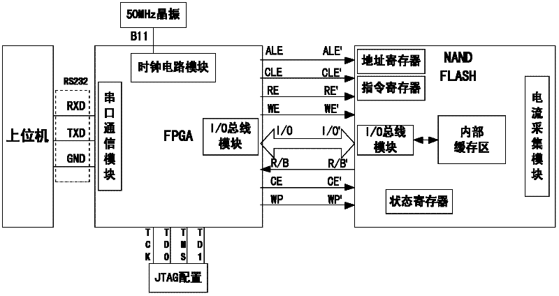
[0124] Such as figure 1 Shown, a kind of FPGA-based NAND FLASH device single event effect test method of the present invention, described method mainly comprises: host computer, 50MHz crystal oscillator, program configuration port JTAG, FPGA control module and NAND FLASH test module; FPGA control module mainly Including serial communication module, clock circuit module and I / O bus module; NAND FLASH test module mainly includes address register, instruction register, internal buffer area, storage unit, status register, I / O bus module and current acquisition module.

[0125] Among them, the upper computer is connected to the FPGA through the data receiving end RXD, the data sending end TXD and the ground wire GND pin of the serial communication RS232 interface; the 50MHz crystal oscillator is connected to the clock signal input end B11 pin of the FPGA to provide an external clock signal for the FPGA; Program configuration port JTAG is connected to FPGA through test clock input s...


PUM


Abstract

The invention discloses an FPGA (Field Programmable Gate Array)-based single event effect test method for a NAND FLASH device and belongs to the field of space radiation effect and reinforcement. The method comprises an upper computer, a 50MHz crystal oscillator, a program configuration port JTAG (Joint Test Action Group), an FPGA control module and an NANF FLASH test module. The test method comprises the following four working modes: 1) static mode; 2) dynamic mode; 3) dynamic reading/ writing mode; and 4) dynamic reading/ erasing/ writing mode. With the method, single event effect test of the large-volume NAND FLASH memory can be realized. Under the condition of an experimental analog source, single event effect characteristic parameters can be efficiently obtained.

Description

technical field [0001] The invention relates to an FPGA-based NAND FLASH device single event effect test method, which belongs to the field of space radiation effect and reinforcement. Background technique [0002] Non-volatile NAND FLASH memory has the characteristics of high storage density, low power consumption, good chip pin compatibility, no data loss after power failure, and no need to refresh data in a short period of time. In recent years, NAND FLASH memory has been widely used in space applications Developed in a trend. [0003] High-energy charged particles in the space environment can induce single event effects in NAND FLASH devices, causing logic errors and abnormal functions, which will have a certain impact on the on-orbit performance of spacecraft payloads. Therefore, the single event effect of NAND FLASH devices Evaluation has been highly valued by designers. Since the structure of NAND FLASH memories above 1G is relatively complex (usually including peri...

Claims


Application Information

Patent Timeline
IPC IPC(8): G11C29/56
Inventor 安恒薛玉雄杨生胜王德坤曹洲把得东石红汤道坦李存惠
Owner NO 510 INST THE FIFTH RES INST OFCHINA AEROSPAE SCI & TECH
Why Eureka
Try Eureka