Inverted lead frame and packaging structure thereof

A flip-chip lead and lead frame technology, applied in electrical components, electrical solid devices, circuits, etc., can solve the problems of abnormally sensitive interconnect resistance, high cost, increased loss, etc., and achieve simple and compact structure, low cost, and reliability. high effect

Inactive Publication Date: 2012-01-25
WUXI CHINA RESOURCE MICRO ASSEMBLY TECH
View PDF10 Cites 2 Cited by
  • Summary
  • Abstract
  • Description
  • Claims
  • Application Information

AI Technical Summary

Problems solved by technology

[0004] However, with the development of electronic technology, more and more IC devices are required to output large current at low voltage. However, the large current output by the packaged chip is extremely sensitive to the interconnection resistance. The higher the interconnection resistance, the more heat Large, the loss increases significantly
It is obviously costly to increase the diameter of the bonded gold wire

Method used


Image

  • Inverted lead frame and packaging structure thereof
  • Inverted lead frame and packaging structure thereof
  • Inverted lead frame and packaging structure thereof

Examples


Embodiment 1

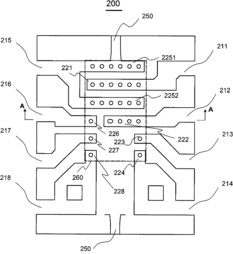
[0035] In the first embodiment, the lead frame of the present invention is described by taking an FCSOIC (Flipchip Small Outline Integrated Circuit Package) lead frame as an example.

[0036] figure 1 Shown is a schematic structural view of the FCSOIC lead frame provided according to the embodiment of the present invention. Such as figure 1 As shown, in this embodiment, the FCSOIC lead frame 200 includes 8 outer pins and 9 inner pins, however, the number of pins of the FCSOIC lead frame is not limited by the embodiments of the present invention, and those skilled in the art can The circuit functionality of the packaged chip requires the selection of a leadframe with a specific number of pins. FCSOIC lead frame 200 is used for flip-chip welding chip (chip die), wherein the region of dotted line frame 260 is the position where the chip is placed after the lead frame of this embodiment is welded and connected to the chip. In this invention, we will figure 1 The shown dotted fr...

Embodiment 2

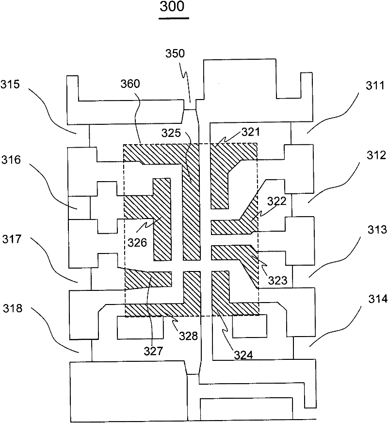
[0049] In the second embodiment, the lead frame of the present invention is described by taking an FCTSOT (Flipchip Thin Small Outline Package, Flip Chip Thin Small Outline Package) lead frame as an example.

[0050] Figure 4 Shown is a schematic structural view of the FCTSOT lead frame provided according to the embodiment of the present invention. Such as Figure 4 As shown, in this embodiment, the FCTSOT lead frame 900 includes 5 inner pins, however, the number of pins of the FCTSOT lead frame is not limited by the embodiment of the present invention, and those skilled in the art can according to the circuit function of the packaged chip Requires to select a leadframe with specific number of pins. The FCTSOT lead frame 900 is used for flip chip welding (chip die), wherein the area of ​​the dotted frame 960 is the position where the chip is placed after the lead frame of this embodiment is welded and connected to the chip. In this invention, we will Figure 4 The shown do...

Embodiment 3

[0059] In the third embodiment, the lead frame of the present invention will be described by taking the lead frame of the Flipchip Thin Quad Flat Non-leaded Package (FCTQFN) as an example.

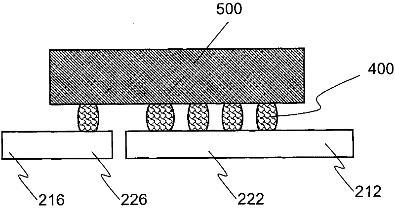
[0060] Figure 7 Shown is a schematic structural view of the FCTQFN lead frame provided according to an embodiment of the present invention; Figure 8 shown as Figure 7 The schematic diagram of the C-C cross-sectional structure after the lead frame packaged chip is formed into the package structure; Figure 9 shown as Figure 7 The schematic diagram of the D-D cross-sectional structure of the lead frame packaged chip after forming the package structure is shown. Such as Figure 8 with Figure 9 As shown, the invention also provides a packaging structure, which includes figure 2 As shown in the lead frame 700 , the packaged chip 500 and the package body 750 , the chip 500 is directly flip-chip soldered to the lead frame 700 through the ball planting point 760 on the pin of the lead ...


PUM


Abstract

The invention provides an inverted lead frame and a packaging structure thereof, belonging to the technical field of chip packaging. The inverted lead frame comprises a first area part corresponding to a position at which a chip to be packaged is placed. The pins of the lead frame are arranged in the first area part at a position corresponding to the position of the pad of the chip on the approximately same plane. The lead frame has the advantages that the structure is simple and compact, the cost is low, the size of the packaging structure formed by the lead frame is small and the packaging requirement of high-output-current chips can be satisfied especially.

Description

technical field [0001] The invention belongs to the technical field of chip packaging, in particular to a lead frame, in particular to a Flipchip (FC) lead frame and its packaging structure. Background technique [0002] Encapsulation is a very important step in the manufacturing process of electronic devices. Through the encapsulation process, various chips (chip die) can be directly drawn out of the circuit, so as to be electrically connected with external circuits. For various chips, the appropriate packaging form is usually selected. [0003] A package structure of a device generally includes a packaged chip, a lead frame and a package (usually a plastic package). Wherein, the lead frame is used to carry the chip and lead out the peripheral interface of the chip to form pins. In the prior art, for various packaging forms, for example, SOIC (SmallOutline Integrated Circuit Package, small outline integrated circuit package) packaging form, TSOT (Thin Small Outline Packag...

Claims


Application Information

Patent Timeline
Patent Type & Authority Applications(China)
IPC IPC(8): H01L23/495H01L25/00
CPCH01L2224/16245
Inventor 郑志荣仲雪梅
Owner WUXI CHINA RESOURCE MICRO ASSEMBLY TECH
Why Eureka
Try Eureka