Method for forming flat dielectric layer

A dielectric layer and flat technology, which is applied in the field of forming a flat dielectric layer, can solve the problem of low yield and achieve the effects of increased yield, reduced thickness difference, and reduced thickness difference

Active Publication Date: 2012-02-01
SHANGHAI HUAHONG GRACE SEMICON MFG CORP
View PDF6 Cites 9 Cited by
  • Summary
  • Abstract
  • Description
  • Claims
  • Application Information

AI Technical Summary

Problems solved by technology

[0006] However, after the above process, the yield of the final device formed at the edge of the wafer is low, only about 38.76%.

Method used


Image

  • Method for forming flat dielectric layer
  • Method for forming flat dielectric layer
  • Method for forming flat dielectric layer

Examples


Embodiment Construction

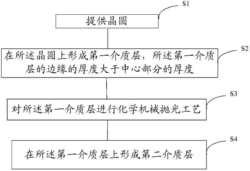
[0034] It can be seen from the background art that the existing method for forming a dielectric layer is to first deposit a dielectric layer by a process such as chemical vapor deposition, and then planarize the surface of the dielectric layer by a chemical mechanical polishing (CMP) process.

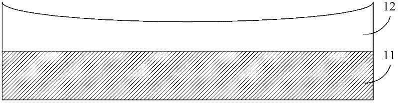
[0035] The inventors have found that the yield of final devices formed at the edge of the wafer is generally lower than the yield of final devices formed at the central portion of the wafer. After further research, the inventor found that after polishing the dielectric layer using the prior art, the thickness of the dielectric layer is not uniform, and the thickness of the dielectric layer at the edge of the wafer is smaller than that of the dielectric layer at the center of the wafer. The thickness of the dielectric layer is small. For example, after chemical mechanical polishing of an 8-inch wafer, due to the different pressures exerted by the grinding head on each part of the wafer, ...


PUM

PropertyMeasurementUnit
thicknessaaaaaaaaaa
thicknessaaaaaaaaaa

Abstract

The invention discloses a method for forming a flat dielectric layer. The method comprises the following steps of: providing a wafer, forming a first dielectric layer on the wafer, wherein the thickness of the edge of the dielectric layer is greater than that of the central part of the dielectric layer; performing chemical and mechanical polishing on the first dielectric layer; and forming a second dielectric layer on the first dielectric layer, wherein the thickness of the edge of the second dielectric layer is greater than that of the central part of the second dielectric layer. For the first dielectric layer formed by the method provided by the embodiment of the invention, the thickness difference between the central part and the edge of the wafer is effectively decreased, and the yield of a final device formed on the edge of the water is effectively improved.

Description

technical field [0001] The invention relates to the field of semiconductor manufacturing, in particular to a method for forming a flat dielectric layer. Background technique [0002] Semiconductor manufacturing processes utilize batch processing techniques that result in the formation of a large number of complex devices on the same wafer. With the rapid development of ultra-large-scale integrated circuits, the integration of chips is getting higher and higher, the size of components is getting smaller and smaller, and the requirements for the accuracy of semiconductor manufacturing processes are getting higher and higher. [0003] In the integrated circuit manufacturing process, after the element structure or patterned metal wires are fabricated on the wafer, a dielectric layer needs to be deposited on it first, and then the subsequent metal layer is deposited. According to different functions, the dielectric layer used to isolate metal wires and components is usually call...

Claims


Application Information

Patent Timeline
Patent Type & Authority Applications(China)
IPC IPC(8): H01L21/31H01L21/311
Inventor 肖海波时廷姜国伟
Owner SHANGHAI HUAHONG GRACE SEMICON MFG CORP
Why Eureka
Try Eureka