4H-SiC ultraviolet photoelectric detector with spherical crown structure, and preparation method
An electrical detector, ultraviolet light technology, applied in circuits, electrical components, semiconductor devices, etc., can solve problems such as affecting quantum efficiency, and achieve the effects of improving detection performance, reducing thickness differences, and increasing absorption angle
- Summary
- Abstract
- Description
- Claims
- Application Information
AI Technical Summary
Problems solved by technology
Method used
Image
Examples
preparation example Construction
[0033] The preparation method of the 4H-SiC ultraviolet photodetector with spherical cap structure comprises the following steps:
[0034] 1) For the sample, that is, a highly doped double-throwing N + Type 4H-SiC substrate and the epitaxially grown i-type absorber layer on the surface are cleaned by RCA standard;
[0035] 2) Preparation of the spherical crown i-type absorbing layer: Combined with the multi-lithographic thick-resist photolithography development technology and ICP etching technology with gradual exposure area, the i-type absorbing layer of the sample was etched multiple times in different ranges to form a series of The arc-shaped table top finally forms the surface of the spherical crown i-shaped absorbing layer.
[0036] 3) Preparation of P + Type layer: A uniformly doped P with a thickness of about 0.2 μm is formed on the upper surface of the spherical crown i-type absorber layer by high-temperature ion implantation process and high-temperature annealing ac...
specific Embodiment
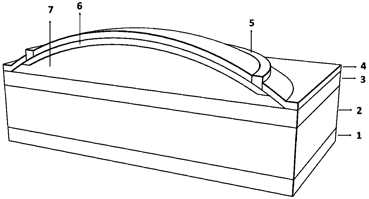
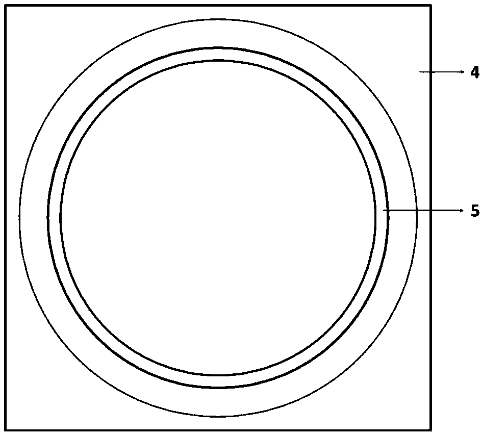
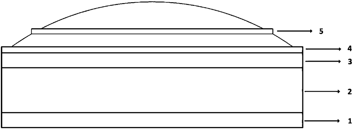
[0047] The structure of the 4H-SiC ultraviolet photodetector with spherical cap structure of the embodiment of the present invention is as follows figure 1 shown. Double-throw N at 4° off-axis with high doping + The N-type buffer layer 3 and the i-type absorber layer 7 are epitaxially and homogeneously grown on the type 4H-SiC substrate 2 in sequence; the thickness and doping concentration of the N-type buffer layer can be 0.5 μm and 5 μm, respectively. ×10 18 / cm 3 , The thickness and doping concentration of the i-type absorbing layer can be 4.0-6.0μm and 1×10 15 / cm 3 ;The i-type absorbing layer is etched into a spherical crown by using the thick-resist lithography process of multiple photolithography plates with gradually changing exposure areas and the ICP dry etching process. The maximum height of the spherical crown can be 4.0-6.0 μm; for the convenience of preparation And quantitatively increase the area of the photosensitive surface and the absorption angle of i...
PUM
 Abstract
Description
Claims
Application Information


