Ferroelectric local field enhanced two-dimensional semiconductor photoelectric detector and preparation method

A two-dimensional semiconductor and local field technology, which is applied in semiconductor/solid-state device manufacturing, semiconductor devices, electric solid-state devices, etc. Issues such as device life or performance, to achieve the effect of improving signal-to-noise ratio and detection ability, reducing dark current, and good stability

Inactive Publication Date: 2016-07-13
SHANGHAI INST OF TECHNICAL PHYSICS - CHINESE ACAD OF SCI
View PDF3 Cites 22 Cited by
  • Summary
  • Abstract
  • Description
  • Claims
  • Application Information

AI Technical Summary

Problems solved by technology

[0004] However, photodetectors based on two-dimensional semiconductors of transition metal chalcogenides will generate high intrinsic carrier concentrations due to their large specific surface area, surface states, and defects. It will lead to high dark current of the device, which seriously restricts the photodetection performance of the device.
In addition, the traditional transition metal chalcogenide compound photodetector needs to apply a constant gate voltage when it works, which will cause high power consumption of the device on the one hand, and also have a certain impact on the stability of the device on the other hand (such as in the electrode area will form hot spots and seriously affect the life or performance of the device), in addition, the band gap of the transition metal chalcogenide two-dimensional semiconductor just falls in the ultraviolet to visible band, which limits the application field of the detector to a certain extent

Method used


Image

  • Ferroelectric local field enhanced two-dimensional semiconductor photoelectric detector and preparation method
  • Ferroelectric local field enhanced two-dimensional semiconductor photoelectric detector and preparation method
  • Ferroelectric local field enhanced two-dimensional semiconductor photoelectric detector and preparation method

Examples


Embodiment Construction

[0039] The specific embodiment of the present invention is described in detail below in conjunction with accompanying drawing:

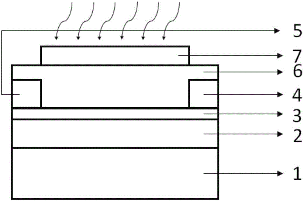
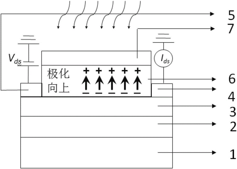
[0040] The invention develops a ferroelectric local field-enhanced two-dimensional semiconductor high-sensitivity photodetector. The ultra-strong local electric field generated by the negative polarization of the P(VDF-TrFE) ferroelectric polymer material completely depletes the intrinsic carriers in the transition metal chalcogenide two-dimensional semiconductor channel, thereby significantly reducing the detection The dark current of the device under no gate voltage improves the detection performance of the device.

[0041] Specific steps are as follows:

[0042] 1. Substrate selection

[0043] A heavily doped p-type silicon with a thickness of 0.5 mm is selected as the substrate.

[0044] 2. Preparation of oxide dielectric layer

[0045] Oxidize silicon dioxide with a thickness of 285 nm on the surface of the silicon substrate by thermal oxida...


PUM


Abstract

The invention discloses a ferroelectric local field enhanced two-dimensional semiconductor photoelectric detector and a preparation method. The detector is characterized in that: the structure of the detector from top to bottom comprises a substrate, a two-dimensional semiconductor, a metal source and drain electrodes, a ferroelectric functional layer and a semi-transparent metal upper electrode in sequence. The preparation method of the detector comprises the steps: a transition-metal chalcogenide two-dimensional semiconductor is prepared on the substrate, an UV lithography or an electron-beam lithography is adopted and combines stripping technology to prepare a metal electrode serving as a source electrode and a drain electrode of a semiconductor channel, a ferroelectric thin film is prepared on the structure, a semi-transparent or transparent electrode is prepared on the ferroelectric thin film, so that a two-dimensional semiconductor detector structure is formed. The detector can make the two-dimensional semiconductor channel background carriers to be completely exhausted through using polarized ferroelectric materials, tiny voltage is applied between the source electrode and the drain electrode, and photoelectric detection is realized through detecting the current signal change under light. The detector has advantages of high sensitivity, fast response, good stability, low power consumption, wide spectrum detection and the like.

Description

technical field [0001] The invention relates to a two-dimensional semiconductor photodetection device, in particular to a ferroelectric local field-enhanced two-dimensional semiconductor photodetector and a preparation method thereof. Background technique [0002] Two-dimensional semiconductors have attracted widespread attention from scientists due to their special series of physical and chemical properties such as force, heat, light, electricity, and magnetism, as well as the peculiar properties of low-dimensional structures. It belongs to the forefront of the research field of new materials and functional devices. Graphene is the origin of two-dimensional material research. Due to its unique two-dimensional characteristics, high light transmission, high carrier mobility and other singular properties, it provides excellent opportunities for high-speed electronic devices and photodetection devices. However, subsequent studies have found that graphene's zero-bandgap charact...

Claims


Application Information

Patent Timeline
Patent Type & Authority Applications(China)
IPC IPC(8): H01L51/42H01L51/46H01L51/48
CPCH10K71/12H10K85/141H10K30/65Y02E10/549Y02P70/50
Inventor 王建禄胡伟达王旭东孙璟兰孟祥建陈效双陆卫褚君浩
Owner SHANGHAI INST OF TECHNICAL PHYSICS - CHINESE ACAD OF SCI
Why Eureka
Try Eureka