MOS device, manufacturing method of MOS device and manufacturing method of CMOS devices

A technology of MOS devices and manufacturing methods, which is applied in the manufacture of semiconductor/solid-state devices, semiconductor devices, electrical components, etc., can solve the problems of affecting the switching speed of devices and the inability to accurately control the thickness of metal gates, so as to reduce parasitic capacitance and save production cost, performance-enhancing effects

Active Publication Date: 2014-02-12
SEMICON MFG INT (SHANGHAI) CORP
View PDF4 Cites 8 Cited by
  • Summary
  • Abstract
  • Description
  • Claims
  • Application Information

AI Technical Summary

Problems solved by technology

For example, in this process, due to the loading effect (Loading effect) and non-uniformity in the chemical mechanical polishing process, etc., the thickness of the metal gate cannot be precisely controlled
In addition, the gate electrode in the prior art has a large parasitic capacitance, which will eventually affect the switching speed of the device, etc.

Method used


Image

  • MOS device, manufacturing method of MOS device and manufacturing method of CMOS devices
  • MOS device, manufacturing method of MOS device and manufacturing method of CMOS devices
  • MOS device, manufacturing method of MOS device and manufacturing method of CMOS devices

Examples


Embodiment Construction

[0060] In order to make the above-mentioned objects, features and advantages of the present invention more obvious and understandable, the specific embodiments of the present invention will be described in detail below with reference to the accompanying drawings.

[0061] In the following description, many specific details are set forth in order to fully understand the present invention, but the present invention can also be implemented in other ways different from those described here, so the present invention is not limited by the specific embodiments disclosed below.

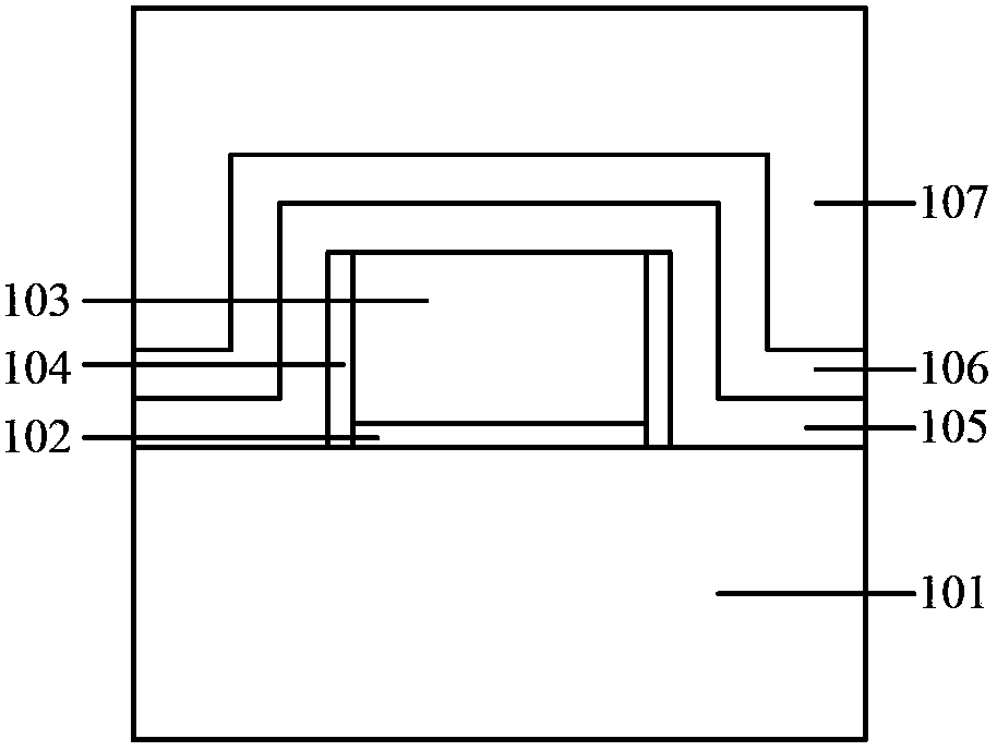
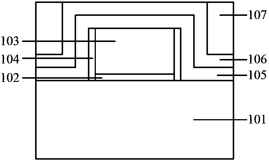
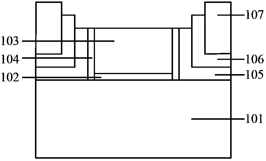
[0062] As mentioned in the background art section, the parasitic capacitance of MOS devices (including CMOS devices) in the prior art is relatively large, and the thickness difference between polysilicon gate and metal gate is relatively large (after multiple etching treatments, the thickness of the metal gate It is about half of the polysilicon gate), resulting in the difficulty of controlling the thickness of the...


PUM


Abstract

The invention provides an MOS device, a manufacturing method of the MOS device and a manufacturing method of two kinds of CMOS devices. The manufacturing method of the MOS device comprises the step of providing a substrate comprising a polysilicon gate, the step of sequentially forming a middle layer, an isolation layer and a first interlayer dielectric layer on the substrate and the polysilicon gate, the step of enabling the upper surface of the first interlayer dielectric layer to be flush with the upper surface of the isolation layer, the step of removing the isolation layer on the polysilicon gate, the middle layer above the polysilicon gate and the polysilicon gate to form a groove, the step of forming a metal grid in the groove, the step of carrying out the planarization processing to enable the upper surface of the metal grid, the upper surface of the first interlayer dielectric layer, the upper surface of the isolation layer and the upper surface of the middle layer to be flush with one another, the step of removing the middle layer on the side wall of the metal grid to form a gap and the step of forming second interlayer dielectric layers on the upper surface of the first interlayer dielectric layer, the upper surface of the isolation layer, the upper surface of the gap and the upper surface of the metal grid. The thickness of the metal grid can be accurately controlled, stray capacitance can be reduced, and the performance of the device can be improved.

Description

Technical field [0001] The present invention relates to the field of semiconductor technology, in particular to a MOS (Metal Oxide Semiconductor) device, a method for manufacturing a MOS device, and a method for manufacturing two CMOS (Complementary Metal Oxide Semiconductor) devices. Background technique [0002] With the continuous development of integrated circuit manufacturing technology, the feature size of MOS devices is getting smaller and smaller. As the feature size of MOS devices continues to shrink, in order to reduce the parasitic capacitance of the gate of the MOS device and increase the speed of the device, a gate stack structure of a high-K gate dielectric layer and a metal gate electrode is introduced into the MOS device. [0003] In order to avoid the influence of the metal material of the metal gate electrode on other structures of the device, the gate stack structure of the metal gate electrode and the high-K gate dielectric layer is usually manufactured by a gat...

Claims


Application Information

Patent Timeline
Patent Type & Authority Applications(China)
IPC IPC(8): H01L21/336H01L21/28H01L21/8238H01L29/78H01L29/423
CPCH01L21/823864H01L29/42356H01L29/66545H01L29/78
Inventor 李凤莲韩秋华倪景华
Owner SEMICON MFG INT (SHANGHAI) CORP
Why Eureka
Try Eureka