Check patentability & draft patents in minutes with Patsnap Eureka AI!

Printed circuit board

A technology of printed circuit boards and circuit substrates, which is applied in the directions of printed circuit components, electrical connection formation of printed components, and electrical connection of printed components, etc., which can solve the problems of increasing the burden of exposure and development processes and complicated processes, and achieve shortened production time and The effect of process cost

Inactive Publication Date: 2012-02-01
NAN YA PRINTED CIRCUIT BOARD CORPORATION
View PDF5 Cites 3 Cited by
  • Summary
  • Abstract
  • Description
  • Claims
  • Application Information

AI Technical Summary

Problems solved by technology

However, this known technology forms copper pillars on the green paint, which requires processes such as coating, exposure, development, and heat treatment. After the green paint layer is completed, the image transfer needs to be performed again on the top of the green paint open ring, and it is matched with electroplated copper. form copper pillars
The process is quite complicated and increases the burden on the exposure and development process

Method used


Image

  • Printed circuit board
  • Printed circuit board
  • Printed circuit board

Examples


Embodiment Construction

[0047] Hereinafter, each embodiment is described in detail and examples accompanied by accompanying drawings are used as a reference basis of the present invention. In the drawings or descriptions of the specification, similar or identical parts all use the same figure numbers, and in the drawings, the shape or thickness of the embodiments may be enlarged and marked in a convenient and simplified manner. Furthermore, the parts of each component in the drawings will be described separately. It should be noted that the components not shown or described in the figure are forms known to those skilled in the art. In addition, specific The examples are only to reveal the specific mode used in the present invention, and are not intended to limit the present invention.

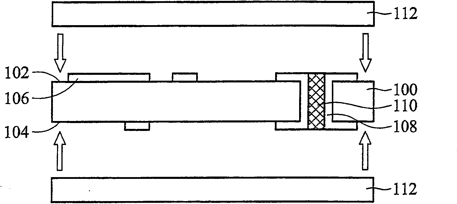
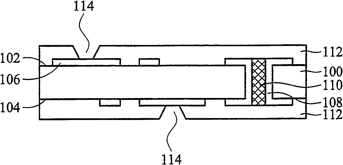
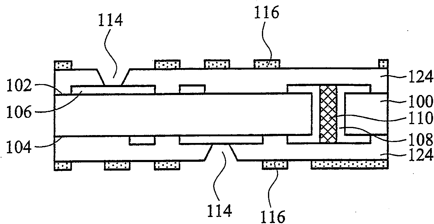
[0048] Figure 1A ~ Figure 1I It is a process sectional view of a printed circuit board according to an embodiment of the present invention. Please refer to Figure 1A, firstly, a circuit substrate 100 is provided, ...


PUM


Abstract

The invention provides a printed circuit board, which comprises a circuit substrate, at least one build-up circuit structure, a top insulating layer, a conductive blind hole and a metal bump, wherein the circuit substrate is provided with a first circuit structure; the build-up circuit structure is arranged on the first circuit structure of the circuit substrate; the top insulating layer is formed on the at least one build-up circuit structure; the conductive blind hole is formed in the top insulating layer; the metal bump is arranged on the conductive blind hole in the top insulating layer; the metal bump and the conductive blind hole have different shapes or sizes. In another embodiment of the invention, a plurality of conductive blind holes are formed in the top insulating layer; a metal bonding pad is formed on a plurality of conductive blind holes; the size of the metal bonding pad is greater than that of the conductive blind holes; and the metal bonding pad is electrically connected with the electrical connection bonding pad of the at least one build-up circuit structure through conductive blind holes. By the invention, the comprehensive production time of the printed circuit board can be shortened, and the process cost can be reduced.

Description

technical field [0001] The invention relates to an electronic component, in particular to a printed circuit board. Background technique [0002] In order to meet the needs of light, thin, short, and small electronic products, the volume of substrates and semiconductor components also needs to be reduced. In addition, due to the high-speed, high-frequency and multi-functional operation requirements of semiconductor components, the number of input and output terminals continues to increase. Therefore, it is necessary to greatly increase the contacts between the printed circuit board and the chip (such as pre-solder bumps) to increase the circuit density of the printed circuit board, but the distance between the contacts must be continuously reduced. However, in the known printed circuit board technology, solder bumps are formed by steel plate opening and solder paste printing, which is limited by the ability of the steel plate to open loops, and solder bridges (solder bridges...

Claims


Application Information

Patent Timeline
Patent Type & Authority Applications(China)
IPC IPC(8): H05K1/02H05K1/11H05K3/42
Inventor 林贤杰傅维达黄皓威
Owner NAN YA PRINTED CIRCUIT BOARD CORPORATION
Features
  • R&D
  • Intellectual Property
  • Life Sciences
  • Materials
  • Tech Scout
  • Unparalleled Data Quality
  • Higher Quality Content
  • 60% Fewer Hallucinations
Learn More